
FRAMOS Functional Adapter (FFA)#
The FRAMOS Functional Adapters (FFA) add device specific functionality to the FSM Ecosystem. They are optional to use and provide PixelMate™ interfaces on in- and output. This way they integrate seamlessly into an existing chain that consists of all components required to connect an FSM to a processor board.

Figure 10: Block Diagram of components in MIPI CSI-2 chain with optional FFA on top FSM chain.
As an example, Figure 10 shows the block diagram of two FSMs connected to a processor board with their appropriate adapters (FSA, FPA). In the lower chain (#2), the FSM+FSA combination is directly connected to the FPA via the generalized PixelMate™ connector. In the upper chain (#1) contains an FFA (pair) with PixelMate™ in- and output. This FFA can be a single PCB performing i.e. image pre-processing, as well as a pair of boards acting as interface adapters, converting the interface completely (SerDes) or partially (connector/cable type) back and forth.
FFA-GMSL-SerDes#
On the FRAMOS Functional Adapters (FFAs) for GMSL, Maxim’s “Gigabit Multimedia Serial Link” is utilized to transfer up to 12 Gbps of uncompressed video data, I2C communication, GPIOs and Power via a single coax wire with automotive grade Fakra connectors.
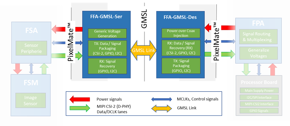
Figure 11: Block Diagram of FFA-GMSL-Ser and FFA-GMSL-Des inside the FSM Ecosystem.
As shown in Figure 11, the integration takes place in form of a serializer- (FFA-GMSL-Ser) and deserializer- (FFA-GMSL-Des) board, that create the appropriate GMSL line between each other and providing PixelMate™ conform MIPI CSI-2 connectivity on in- / output to FSA / FPA. This way they are physically compatible to all FSMs of the Ecosystem with this interface.
Note: Due to high power requirements of specific sensors, even if physically interface compatible, operation might not be possible due to lack of power over coax. Please check the Table 14 for an overview about tested and confirmed setups.
[Full Resolution / | max. FPS] | |
||||
|---|---|---|---|---|
Modules |
Physically Compatible |
Reference Drivers (NVIDIA Jetson)** |
6 Gbps Driver support on request, physically supported. |
12 Gbps |
FSM-AR0144 |
Yes |
On Request |
||
FSM-AR0521 |
Yes |
On Request |
||
FSM-AR1335 |
Yes |
On Request |
||
FSM-HDP230 |
Yes |
On Request |
||
FSM-IMX264 |
Yes |
On Request |
||
FSM-IMX283 |
Yes |
On Request |
||
FSM-IMX290 |
Yes |
Yes |
1920 x 1080 / 120 |
|
FSM-IMX327 |
Yes |
On Request |
||
FSM-IMX296 |
Yes |
Yes |
1456 x 1088 / 60 |
|
FSM-IMX297 |
Yes |
On Request |
||
FSM-IMX304 |
Yes[1] |
Yes |
4112 x 3008 / 24 |
|
FSM-IMX334 |
Yes |
On Request |
||
FSM-IMX335 |
Yes |
On Request |
||
FSM-IMX412 |
Yes |
Yes |
4056 x 3040 / 60 |
|
FSM-IMX477 |
Yes |
On Request |
||
FSM-IMX577 |
Yes |
Yes |
4056 x 3040 / 60 |
|
FSM-IMX415, 715 |
Yes |
Yes |
3864 x 2192 / 90 |
|
FSM-IMX462 |
Yes |
Yes |
1920 x 1080 / 120 |
|
FSM-IMX662 |
Yes |
Yes |
1920 x 1080 / 98 |
|
FSM-IMX464 |
Yes |
Yes |
2712 x 1538 / 90 |
|
FSM-IMX485 |
Yes |
On Request |
||
FSM-IMX568 |
Yes |
Yes |
2472 x 2064 / 96 |
|
FSM-IMX585 |
Yes |
Yes |
3856 x 2180 / 90 |
|
FSM-IMX530 |
Yes[2] |
Yes |
5328 x 4608 / 15 |
|
FSM-IMX565 |
Yes |
Yes |
4128 x 3008 / 43 |
|
FSM-IMX675 |
Yes |
Yes |
2608 x 1964 / 81 |
|
FSM-IMX678 |
Yes |
Yes |
3856 x 2180 / 72 |
|
FSM-IMX990 |
Yes |
Yes |
1296 x 1032 / 125 |
|
Table: FRAMOS Sensor Module Compatibility and Support by FFA-GMSL-SerDes
Note: With the revision V1A of the FFA-GMSL-Des (Deserializer), only one GMSL line is supported per carrier board. The power supplied from the carriers is not sufficient to source multiple or demanding image sensors. The V2A variant supports more power demanding image sensors with an external 12V power supply.
Latency
The latency added by GMSL conversion is related to the data rate and image width. It is 1 video line + 128 x TPCLK where TPCLK is the pixel clock of the sensor. As the actual delay depends on the operation mode, you can find a few examples for orientation below.
Modules |
Resolution [V x H] |
Framerate [fps / Hz] |
Latency [µs] |
|---|---|---|---|
FSM-IMX462 |
1920 x 1080 |
60 120 |
7,76 8,26 |
FSM-IMX415 |
3864 x 2192 |
45 90 |
23,55 10,15 |
FSM-IMX283 |
5496 x 3694 |
12 25 |
47,21 31,58 |
The values needed for calculation can be found in the corresponding sensor datasheet.
Sensor Communication and General Purpose Input- / Outputs (GPIO)
The SerDes chain embeds several (sensor) signals as well as communication into the GMSL stream. It is differentiated between 10 available multi-functional pins (MFP), providing latency optimized signals, and slower signals available by an IO extender communicating via I2C:
GPIO Extender:
SLAMODE0, SLAMODE1, SLAMODE2, XMASTER, TOUT0, TOUT1, TOUT2
Multi-Functional Pins
MFP0: SCK
MFP1: XCE
MFP2: XCLR
MFP3: XVS
MFP4: INCK (MFP4 is output of PLL, can generate a 1-75 MHz clock)
MFP5: XHS (OD out)
MFP6: XTRIG1 (OD out)
MFP7: SDI or I2C SDA (configurable)
MFP8: SDO or I2C SCL (configurable)
MFP9: XTRIG2 (OD out)
MFP10: NC
For details on the specific signals, check the documentation of your image sensor and FSA type.
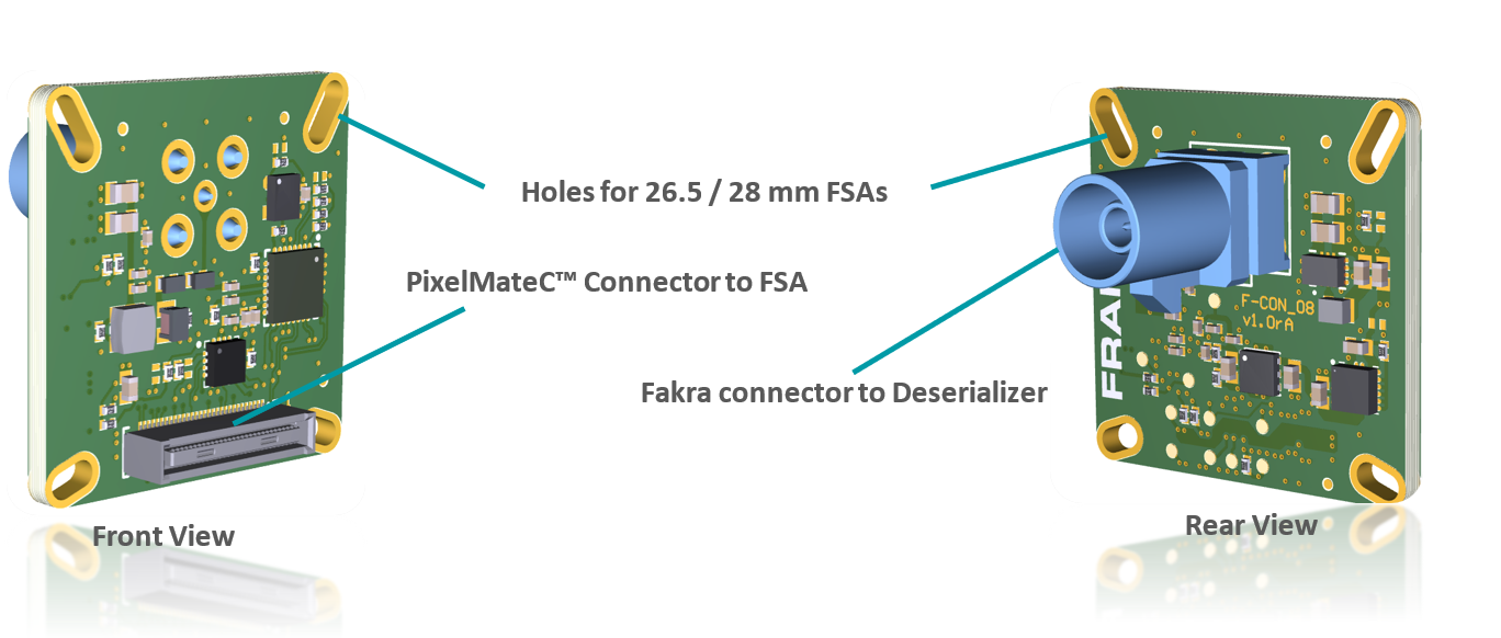
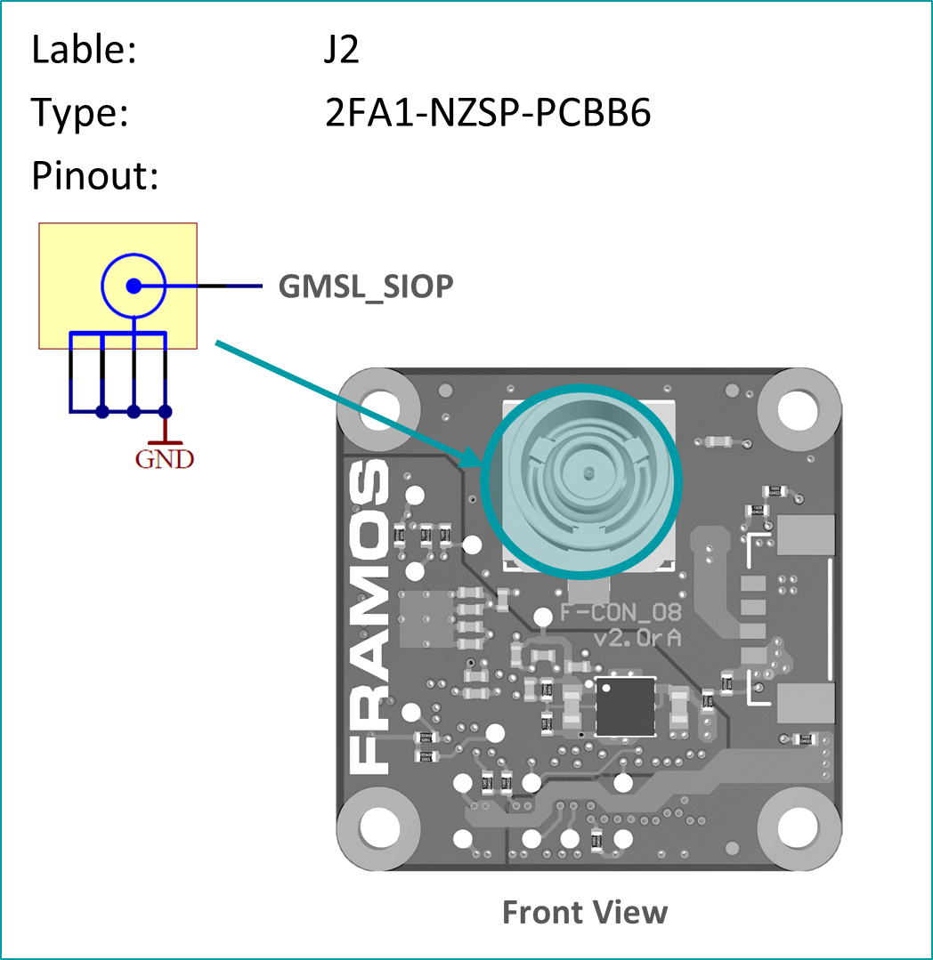
FFA-GMSL-Ser-V1A (Serializer, Sensor Side)#
Serializer board acting as transmitter (TX), connecting to FSM+FSA stack serializing image data, embedding of bidirectional communication and sensor GPIOs. Connects to PixelMateC and outputs GMSL on Fakra type connector.
4-Lane MIPI CSI-2 Input
Supporting 6 / 12 Gbps output modes
Generic supply voltage (3V8, 1V8) recovery from PoC
GPIOs and I2C Communication via MFP/ I2C Extender
Testpoints to important signals
Compatible to GMSL 6 / 12 Gbps compliant receivers.
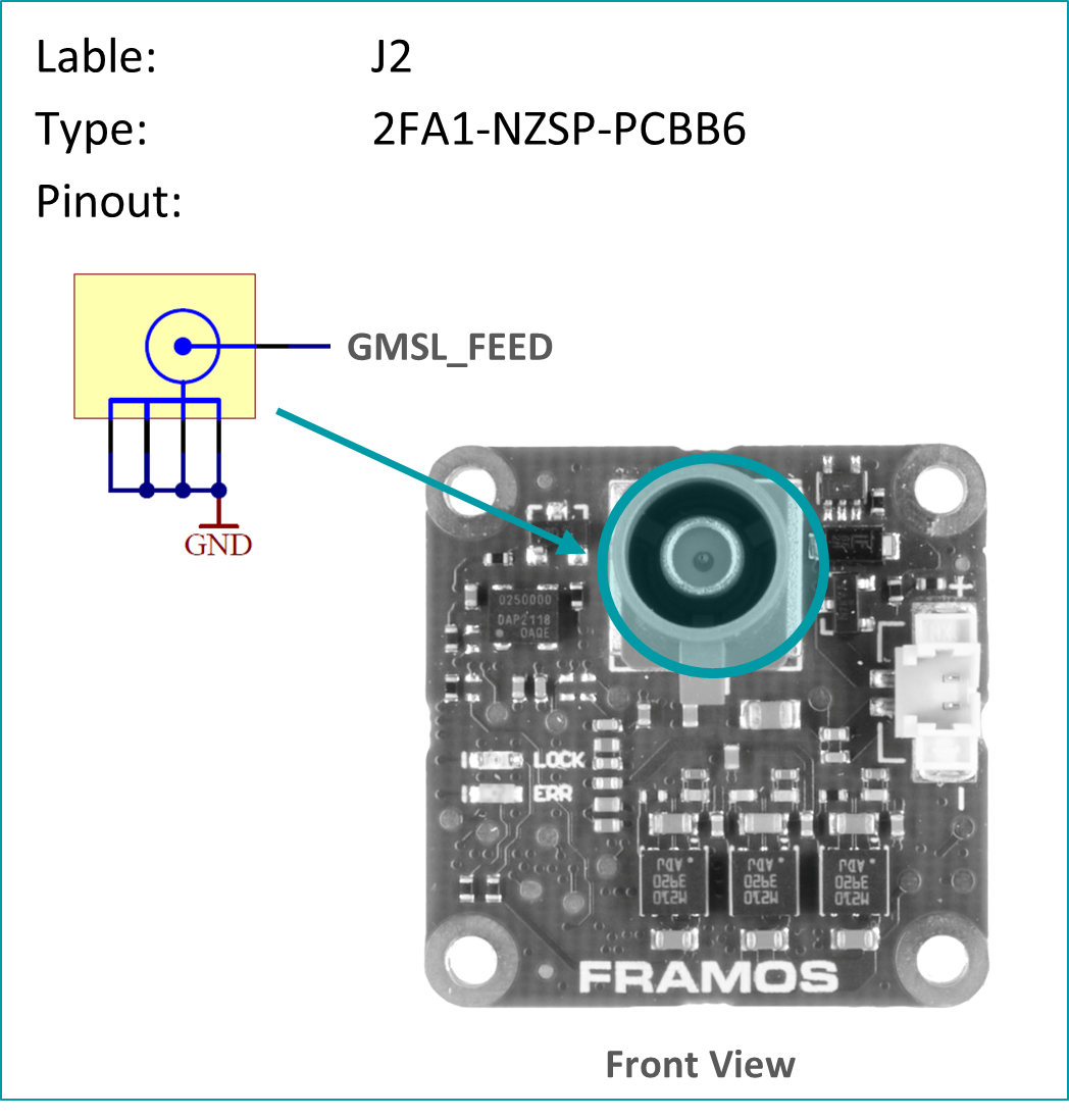
Fakra / GMSL Connector

PixelMateC™ Connector
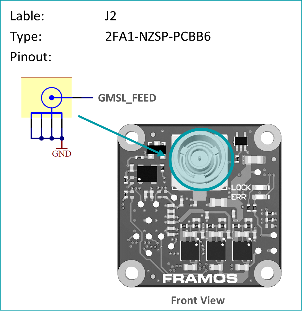
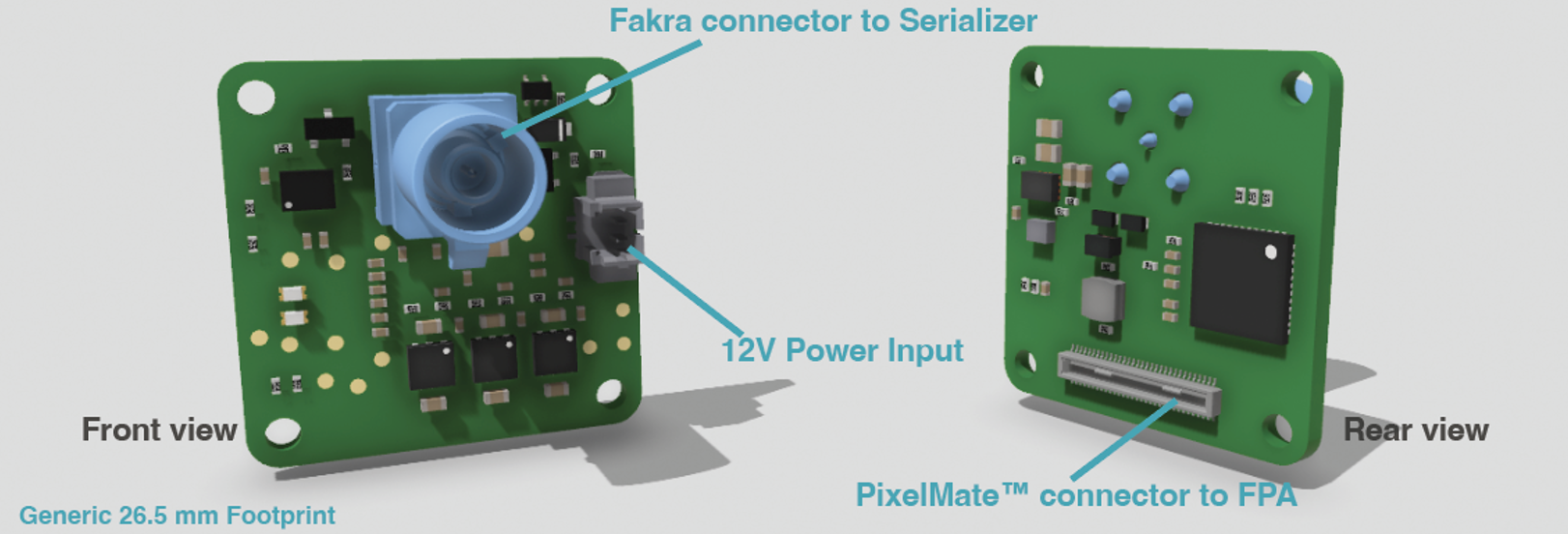
FFA-GMSL-Ser-V2A (Serializer, Sensor Side)#
Serializer board acting as transmitter (TX), connecting to FSM+FSA stack serializing image data, embedding of bidirectional communication and sensor GPIOs. Connects to PixelMateC and outputs GMSL on Fakra type connector.
4-Lane MIPI CSI-2 Input
Supporting 6 / 12 Gbps output modes
Generic supply voltage (3V8, 1V8) recovery from PoC
V2A: 26.5 mm footprint [2]_
GPIOs and I2C Communication via MFP/ I2C Extender
Testpoints to important signals
Compatible to GMSL 6 / 12 Gbps compliant receivers.
Fakra / GMSL Connector
PixelMateC™ Connector
FFA-GMSL-Des-V1A (Deserializer, Processor Side)#
The deserializer board acts as a receiver (RX) by converting GMSL data (on the input) to FPA or Carrier boards using the PixelMateC interface. This board comes in two variants, namely FFA-GMSL-Des-V1A and FFS-GMSL-Des-V2A, both of which are responsible for deserializing image data, embedding bidirectional communication, and sensor GPIOs. They connect to the PixelMateC interface and output GMSL through a Fakra-type connector. The key features of the deserializer board are listed below, along with the differences between the V1A and V2A variants.
Supporting 6 / 12 Gbps input modes
4-Lane MIPI CSI-2 Output
Maximum one GMSL chain supported per FPA/Carrier
- GPIOs and I2C Communication viaMFP / I2C Extender
Testpoints to important signals
Power over Coax (PoC) Injection

Fakra / GMSL Connector
PixelMateC™ Connector
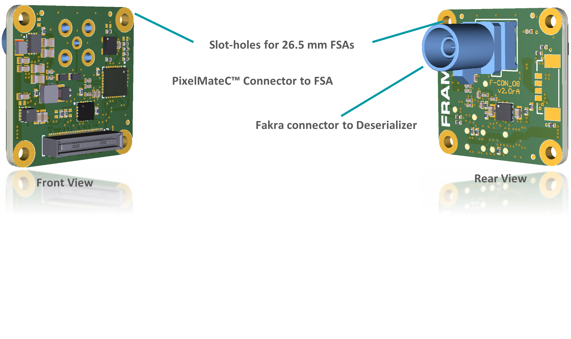
FFA-GMSL-Des-V2A (Deserializer, Processor Side)#
The deserializer board acts as a receiver (RX) by converting GMSL data (on the input) to FPA or Carrier boards using the PixelMateC interface. This board comes in two variants, namely FFA-GMSL-Des-V1A and FFS-GMSL-Des-V2A, both of which are responsible for deserializing image data, embedding bidirectional communication, and sensor GPIOs. They connect to the PixelMateC interface and output GMSL through a Fakra-type connector. The key features of the deserializer board are listed below, along with the differences between the V1A and V2A variants.
Supporting 6 / 12 Gbps input modes
4-Lane MIPI CSI-2 Output
Power over Coax (PoC) Injection
V2A variant allows a separate, carrier independent power input
- GPIOs and I2C Communication viaMFP / I2C Extender
Testpoints to important signals
Supports multi-sensor operation on the FPA/Carrier
Fakra / GMSL Connector
PixelMateC™ Connector
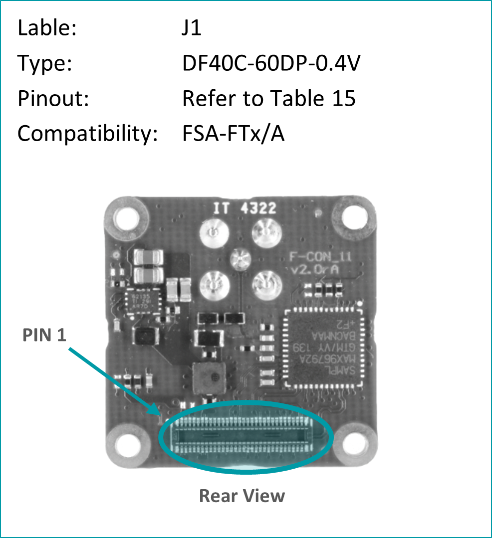
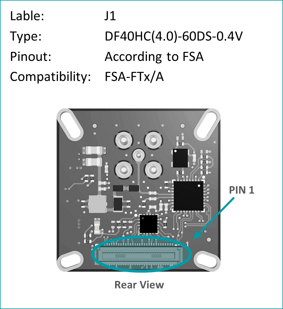
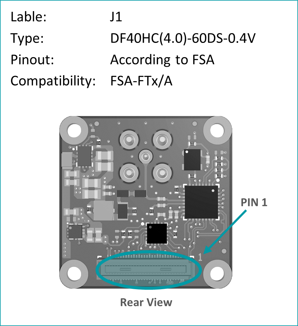
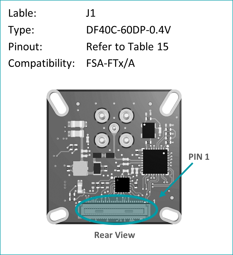
Pinout: J1 (PixelMateC)
Pin # |
Name |
Pin # |
Name |
|---|---|---|---|
1 |
3V8_VDD |
2 |
1V8_VDD |
3 |
3V8_VDD |
4 |
1V8_VDD |
5 |
NC |
6 |
NC |
7 |
NC |
8 |
NC |
9 |
NC |
10 |
NC |
11 |
GND |
12 |
GND |
13 |
GND |
14 |
GND |
15 |
RST_0 |
16 |
RST_1 |
17 |
NC |
18 |
NC |
19 |
NC |
20 |
NC |
21 |
I2C_0_SCL(SPI_SCK) |
22 |
NC |
23 |
NC |
24 |
NC |
25 |
GPIO1(XVS0) |
26 |
NC |
27 |
I2C_0_SDA(SPI_MOSI) |
28 |
NC |
29 |
GPIO2(XHS0) |
30 |
GPIO10(XTRIG1) |
31 |
GPIO3(XTRIG0) |
32 |
NC |
33 |
PW_EN_0 |
34 |
PW_EN_1 |
35 |
NC |
36 |
NC |
37 |
GND |
38 |
GND |
39 |
MCLK_0 |
40 |
NC |
41 |
NC |
42 |
NC |
43 |
GND |
44 |
GND |
45 |
NC |
46 |
D_DATA_3_P |
47 |
NC |
48 |
D_DATA_3_N |
49 |
GND |
50 |
GND |
51 |
D_DATA_0_N |
52 |
D_DATA_1_N |
53 |
D_DATA_0_P |
54 |
D_DATA_1_P |
55 |
GND |
56 |
GND |
57 |
D_DATA_2_P |
58 |
D_CLK_0_P |
59 |
D_DATA_2_N |
60 |
D_CLK_0_N |
Table 15: Pinout of FFA-GMSL-Des-VXA, connector to FRAMOS Processor Adapter (FPA)
Device Details:
The FFA-GMSL-Des-V2A deserializer is similar to the V1A variant. However, it moves the PoC power source to an external power supply, making it independent of power limitations imposed by the FPA or carrier board. As a result, it can support demanding sensors as well as multi-sensor operation on the FPA/Carrier, whereas the V1A variant only supports one sensor. One GMSL deserializer physically supports 6 or 12 Gbps GMSL input, and one MIPI CSI-2 output via PixelMate™. The V2A deserializer receives power from a required external 12V power supply before being converted down by a switching buck converter to 8V, which is then available through Power over Coax (PoC):
Note: To provide power to the V2A deserializer, an external 12 V power supply is required. A power rating of 12 VDC, 1 A is recommended.
It is important to note that though 6 Gbps is physically supported in the V2A variant of the deserializer, NVIDIA Jetpack JP5.1 only supports the 12 Gbps speed.
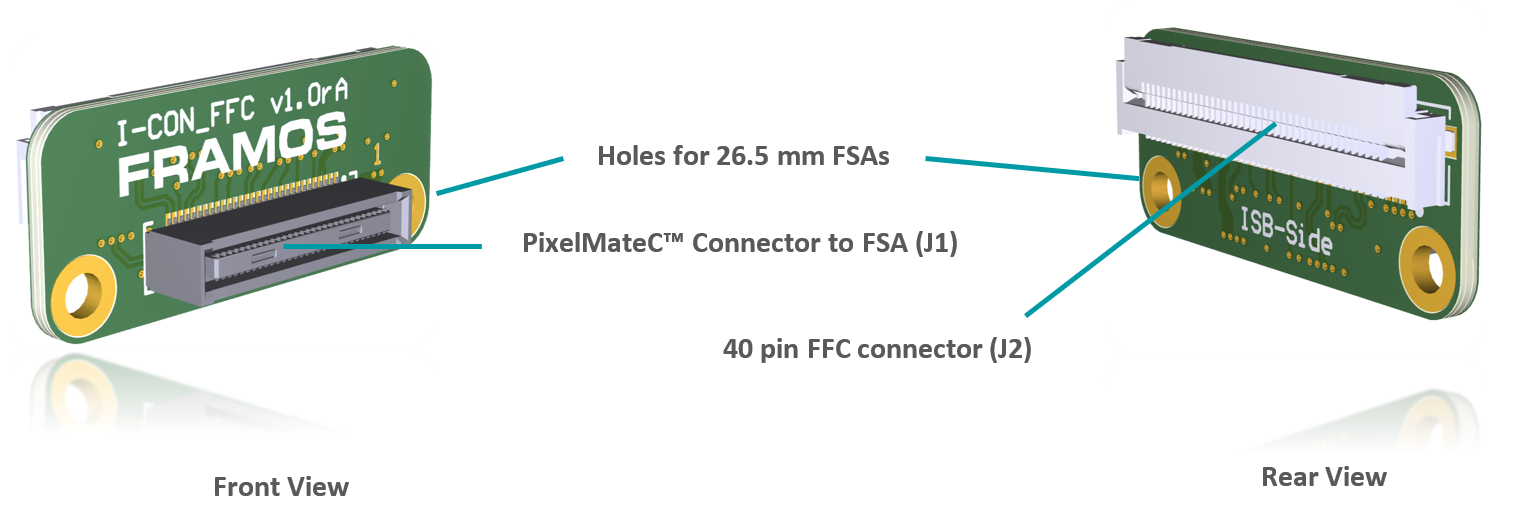
FFA-FFC – PixelMateC to FFC Adapters#
Two small format boards (FFA-A/FFC and FFA-FFC/A) are available which adapt the PixelMateC MIPI CSI-2 connector to an unshielded Flat Flexible Cable (FFC) and back. This allows the connection of affordable and highly available FFC cabling in different lengths between the front-end and the receiver for evaluation purposes and as reference for integrated solutions on custom basis.
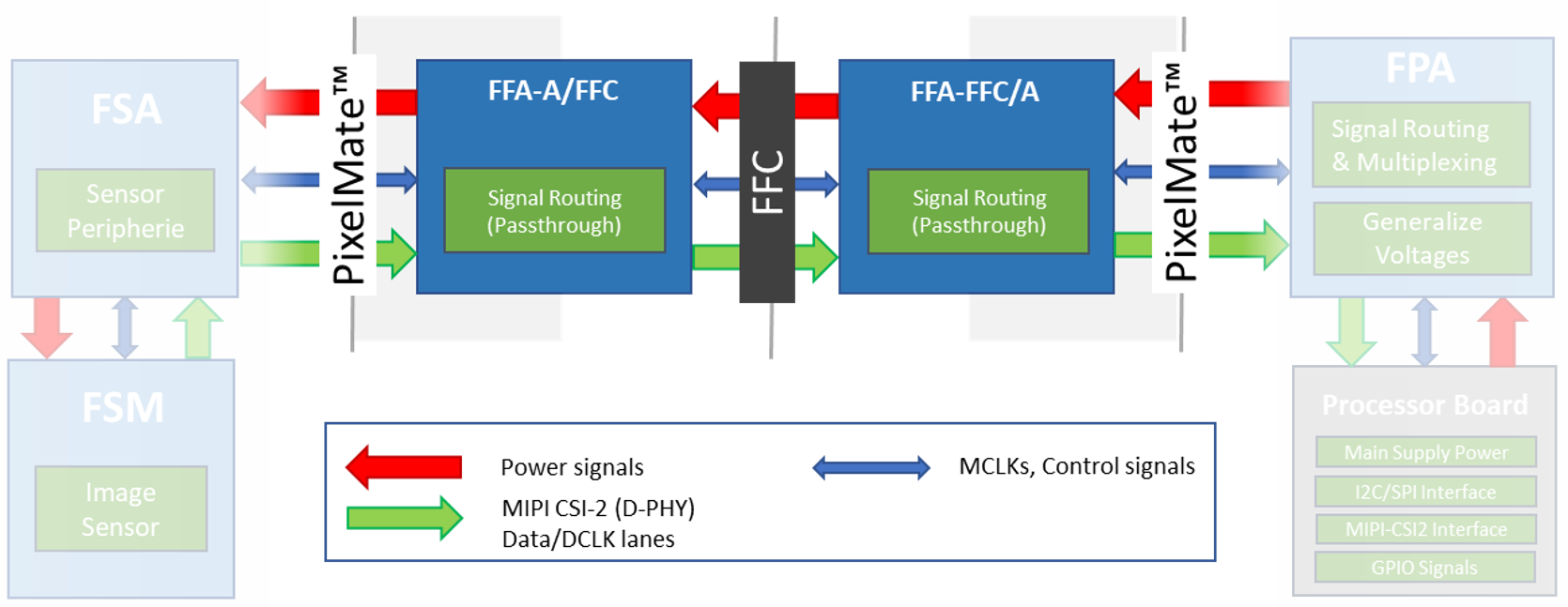
Figure: System Diagram of FFA-A/FFC and FFA-FFC/A inside the FSM Ecosystem.
As shown in the above figure, the integration takes place in form of two FFAs, adapting from PixelMateC to FFC and back. The boards only take care about signal routing from one to the other connector, signals pass through and stay unaltered.
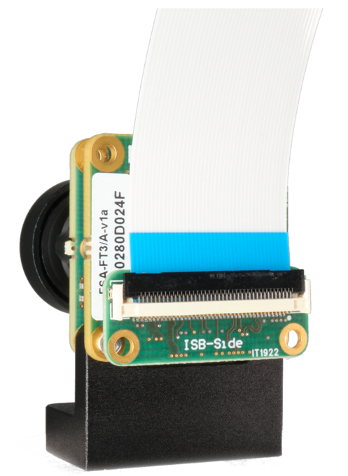
Figure: FFA-A/FFC Connected to FSM+FSA Stack (Front-End)
Cabling
For the cabling, an unshielded standard 40 pin FFC cable with 0.5 mm pitch is required. For signal matching, a TOP to BOTTOM cable (like the Molex 0150200440 or 0150200446) must be used in-between both adapters.
Due to the reduction from 60 pins to 40 pins, a couple of signals were dropped from the PixelMateC layout. The following signals are not available when using the FFC cable:
RST1 (1)
Second I2C (2)
MCLK 1, 2, 3 (3)
GPIOs: 14, 15, 8, 17, 9, 10, 11 (7)
SLAMODE 1, 2, 3 (3)
Second MIPI CLK (2)
GND (2)
Regular single sensor setups in the FSM Ecosystem (native CSI-2 or converted from SLVS) do not use these signals and are not affected by missing signals. The complete pinout can be found in the following adapter-specific chapters.
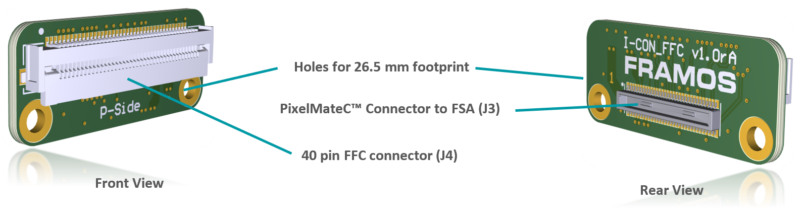
FFA-A/FFC40-V1A (PixelMateC to 40 pin FFC, Sensor / FSA Side)#
The FFA-A/FFC40 board adapts the output of the front-end (FSM+FSA stack) to utilize an appropriate FFC cable. The pin count is reduced from 60 pins to 40 pins; signals stay untouched.
FFC Connector |
|||||
|---|---|---|---|---|---|
Label: J2 Type: Molex 5051104091 Pin Count: 40 pin Pitch: 0.5 mm Shielding Connector / Cable: No / No |
|||||
|
1 |
GND |
21 |
GPIO3(XTRIG0) |
|
2 |
D_CLK_0_N |
22 |
GPIO2(XHS0) |
||
3 |
D_CLK_0_P |
23 |
GPIO1(XVS0) |
||
4 |
GND |
24 |
I2C_0_SDA(SPI_MOSI) |
||
5 |
D_DATA_2_N |
25 |
I2C_0_SCL(SPI_SCK) |
||
6 |
D_DATA_2_P |
26 |
GPIO0(XMASTER0) |
||
7 |
GND |
27 |
RST_0 |
||
8 |
D_DATA_1_P |
28 |
AUX_V |
||
9 |
D_DATA_1_N |
29 |
AUX_IF |
||
10 |
GND |
30 |
AUX_DIG |
||
11 |
D_DATA_0_P |
31 |
AUX_DIG |
||
12 |
D_DATA_0_N |
32 |
AUX_ANA |
||
13 |
GND |
33 |
AUX_ANA |
||
14 |
D_DATA_3_N |
34 |
GND |
||
15 |
D_DATA_3_P |
35 |
1V8_VDD |
||
16 |
GND |
36 |
1V8_VDD |
||
17 |
MCLK_0 |
37 |
GND |
||
18 |
GND |
38 |
3V8_VDD |
||
19 |
PW_EN_1 |
39 |
3V8_VDD |
||
20 |
PW_EN_0 |
40 |
GND |
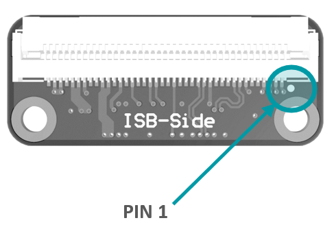
Table: FFC Connector on FFA-A/FFC40
FFA-FFC40/A-V1A (40 pin FFC to PixelMateC, Processor Side)#
Adapting the FFC cable coming from a front-end with FFA-A/FFC back to PixelMateC.
FFC Connector |
|||||
|---|---|---|---|---|---|
Label: J4 Type: Molex 5051104091 Pin Count: 40 pin Pitch: 0.5 mm Shielding Connector / Cable: No / No |
|||||
|
1 |
GND |
21 |
GPIO3(XTRIG0) |
|
2 |
D_CLK_0_N |
22 |
GPIO2(XHS0) |
||
3 |
D_CLK_0_P |
23 |
GPIO1(XVS0) |
||
4 |
GND |
24 |
I2C_0_SDA(SPI_MOSI) |
||
5 |
D_DATA_2_N |
25 |
I2C_0_SCL(SPI_SCK) |
||
6 |
D_DATA_2_P |
26 |
GPIO0(XMASTER0) |
||
7 |
GND |
27 |
RST_0 |
||
8 |
D_DATA_1_P |
28 |
AUX_V |
||
9 |
D_DATA_1_N |
29 |
AUX_IF |
||
10 |
GND |
30 |
AUX_DIG |
||
11 |
D_DATA_0_P |
31 |
AUX_DIG |
||
12 |
D_DATA_0_N |
32 |
AUX_ANA |
||
13 |
GND |
33 |
AUX_ANA |
||
14 |
D_DATA_3_N |
34 |
GND |
||
15 |
D_DATA_3_P |
35 |
1V8_VDD |
||
16 |
GND |
36 |
1V8_VDD |
||
17 |
MCLK_0 |
37 |
GND |
||
18 |
GND |
38 |
3V8_VDD |
||
19 |
PW_EN_1 |
39 |
3V8_VDD |
||
20 |
PW_EN_0 |
40 |
GND |
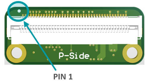
Table: FFC Connector on FFA-FFC40/A
FFA-MC – PixelMateC to Micro Coax Adapters#
Small format boards adapting from the sophisticated PixelMateC MIPI CSI-2 connector to a shielded micro coaxial cable and back. Allowing the connection of special customized, flexible and round cabling made for cable routing through challenging and winding enclosures at great environmental robustness. As a component of the FSM Ecosystem, they aim for evaluation purpose and are a reference to be integrated into custom solutions.
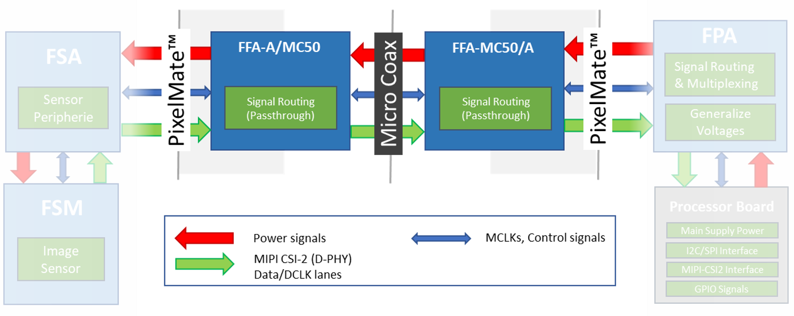
Figure: System Diagram of FFA-A/MC50 and FFA-MC50/A inside the FSM Ecosystem.
As shown in Figure 11, the integration takes place in form of two FFAs, adapting from PixelMateC to micro coax and back. The boards only take care about signal routing from one to the other connector, signals pass through and stay unaltered.
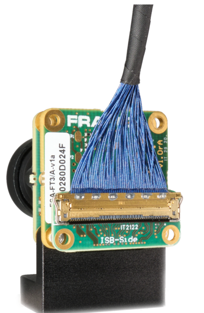
Figure: FFA-A/MC50 Connected to FSM+FSA Stack (Front-End)
Cabling
For the cabling, a shielded, 50 pin micro coaxial cable with 0.4 mm pitch and 1:1 pin assignment on both ends is required. Please refer to Chapter 9.3.3 – “FMA-CBL-MC50-0.3m-V1A – Micro Coax Cable” for a recommended reference assembly.
Due to the reduction from 60 to 50 pins, a couple of signals are dropped from the PixelMateC layout. The following signals are not available:
Second I2C (2)
MCLK 1, 2, 3 (3)
Second MIPI CLK (2)
GND (3)
Regular single sensor setups in the FSM Ecosystem (native CSI-2 or converted from SLVS) do not use these signals and are not affected by missing signals. The complete pinout can be found in the following, adapter specific, chapters.
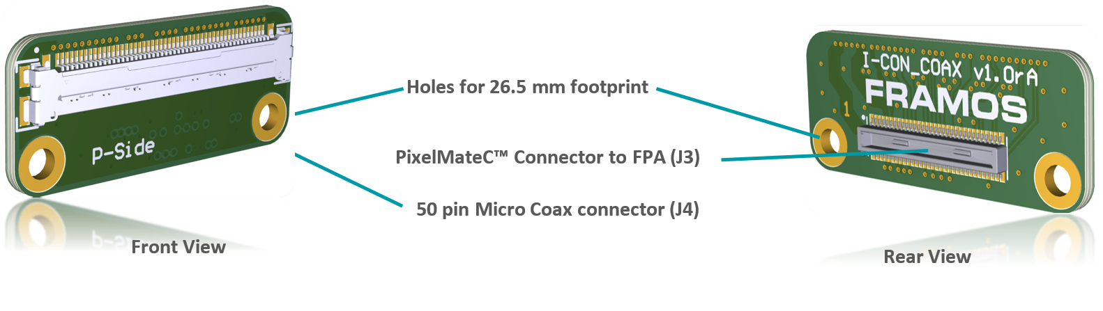
FFA-A/MC50-V1A (PixelMateC to 50 pin Micro Coax, Sensor / FSA Side)#
Adapting the output of the front-end (FSM+FSA stack) to utilize an appropriate Micro Coax cable. Pin count is reduced from 60 pins to 50 pins, signals stay untouched.
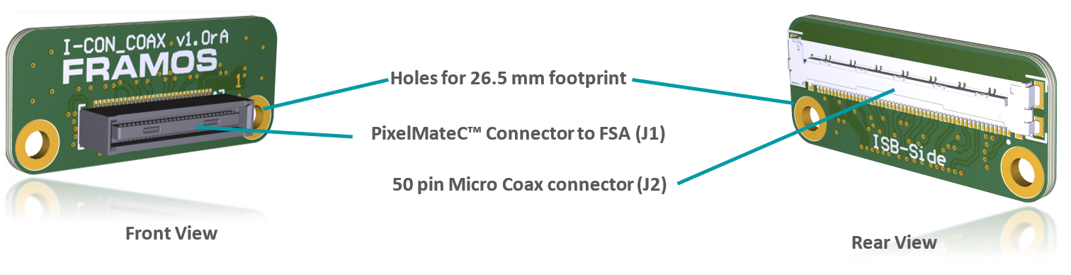
Table: FFC Connector on FFA-A/MC50
FFA-MC50/A-V1A (50 pin FFC to PixelMateC, Processor Side)#
Adapting the output of the front-end (FSM+FSA stack) to utilize an appropriate Micro Coax cable. Pin count is reduced from 60 pins to 50 pins, signals stay untouched.
FFC Connector |
|||||
|---|---|---|---|---|---|
Label: J4 Type: I-PEX 20525-050E-02 Pin Count: 50 pin Pitch: 0.4 mm Shielding: Yes |
|||||
|
1 |
GND |
26 |
I2C_0_SDA(SPI_MOSI) |
|
2 |
D_CLK_0_N |
27 |
GPIO9 |
||
3 |
D_CLK_0_P |
28 |
GPIO1(XVS0) |
||
4 |
GND |
29 |
GPIO16(SYS_PW_EN) |
||
5 |
D_DATA_2_N |
30 |
GPIO17(SPI_CS) |
||
6 |
D_DATA_2_P |
31 |
I2C_0_SCL(SPI_SCK) |
||
7 |
GND |
32 |
GPIO8 |
||
8 |
D_DATA_1_P |
33 |
GPIO0(XMASTER0) |
||
9 |
D_DATA_1_N |
34 |
GPIO15(SPI_MISO) |
||
10 |
GND |
35 |
GPIO14 |
||
11 |
D_DATA_0_P |
36 |
RST_1 |
||
12 |
D_DATA_0_N |
37 |
RST_0 |
||
13 |
GND |
38 |
GND |
||
14 |
D_DATA_3_N |
39 |
AUX_V |
||
15 |
D_DATA_3_P |
40 |
AUX_IF |
||
16 |
GND |
41 |
AUX_DIG |
||
17 |
MCLK_0 |
42 |
AUX_DIG |
||
18 |
GPIO7 |
43 |
AUX_ANA |
||
19 |
GPIO6 |
44 |
AUX_ANA |
||
20 |
PW_EN_1 |
45 |
GND |
||
21 |
PW_EN_0 |
46 |
1V8_VDD |
||
22 |
GPIO11 |
47 |
1V8_VDD |
||
23 |
GPIO3(XTRIG0) |
48 |
GND |
||
24 |
GPIO10 |
49 |
3V8_VDD |
||
25 |
GPIO2(XHS0) |
50 |
3V8_VDD |
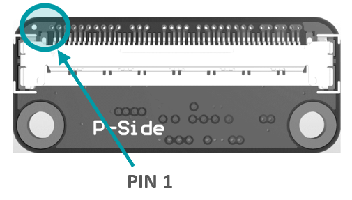
Table: FFC Connector on FFA-FFC40/A
FMA-CBL-MC50-0.3m-V1A – Micro Coax Cable#
Cable assembly of I-PEX connectors with micro coaxial cable. CE and RoHS compliant, various lengths are available on request. Pin assignment is 1:1.
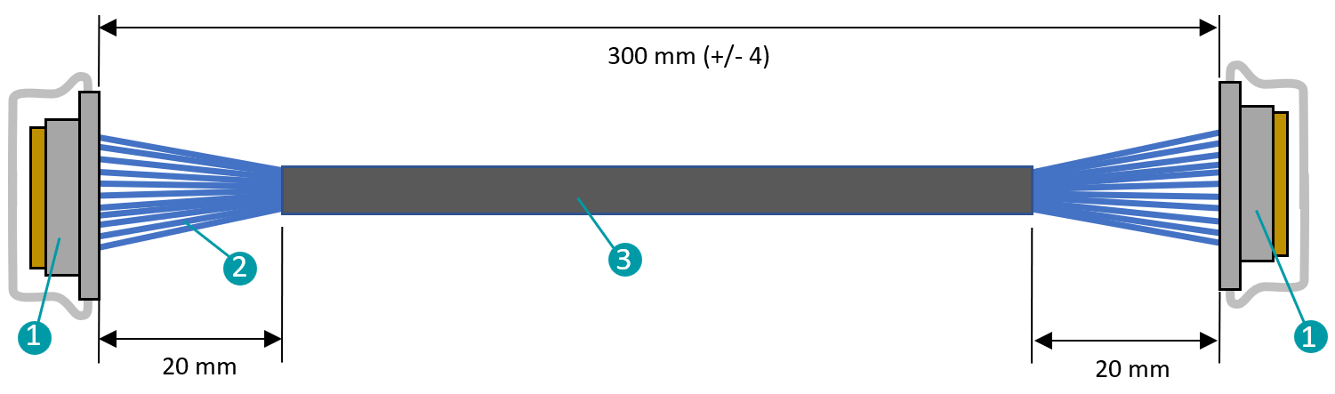
Connector: I-PEX CABLINE® -CA
Housing: 20634-150T-02
Shell: 2764-0501-002
P-Bar: 2766-0501
Shielded: Yes
Contact Pitch (mm): 0.400
Height: 1.10 Max (1.00 Nom.)
Pin Count: 50
Mating Direction: Horizontal
Cable: Micro Coaxial
Type: MCX AWG40 UL1354
Length: 300 mm
Color: Black
Insulation Tape