
FRAMOS Processor Adapter (FPA)#
Connects multiple FSAs to one processor board
Processor board specific
Differentiates two input interface types:
A: MIPI CSI-2
BC: Sub-LVDS / SLVS (B) and SLVS-EC (C)
FPA-4.A/AGX-V1A: Quad FPA to NVIDIA Jetson AGX Orin and AGX Xavier#
Adapting from PixelMate to NVIDIA Jetson AGX Developer Kit Connector
Four 4-Lane MIPI CSI-2
Generation of standard PixelMate power rails
Testpoints to important sensor signals
Enhanced sensor control signal access via I2C extender
Synchronization and timing signal access via Molex Picoblade connector
Compatible Processor Boards:
NVIDIA Jetson Orin AGX Development Kit
NVIDIA Jetson Xavier AGX Development Kit

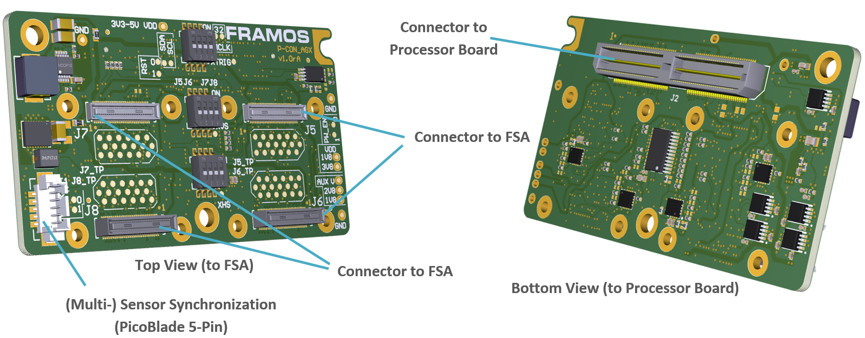
Description of Connectors and Interfaces#
Name |
Description |
Connector Type |
Orientation |
|---|---|---|---|
J1 |
XVS, XHS and XTRIG Signals |
Molex PicoBlade, 5-Pin (53398-0571) |
Pin 1 marked on PCB |
J2 |
PixelMate to Processor Board |
Samtec QTH-060-01-L-D-A |
Pin 1 marked on PCB |
J5 |
PixelMate to FSA (4x MIPI CSI-2 lanes) |
Hirose DF40C-60DS-0.4V(51) |
Pin 1 Printed on PCB next to each connector. |
J6 |
Hirose DF40H C(4.0)-60DS-0.4V(51) |
||
J7 |
Hirose DF40C-60DS-0.4V(51) |
||
J8 |
Hirose DF40H C(4.0)-60DS-0.4V(51) |
Table: Connectors on FPA-4.A/AGX-V1A
The Pin 1 markings can be found in the following chapters along with the Pinout, as well as on the PCB in copper or silkscreen layer next to the connector.
Note: All signals are routed from J5, J6, J7, J8 (to FSA) to J2 (to processor), test points and pin row. They follow the signal specification according to the FSA output interface. Control signals going to J1 (I2C, clock, GPIO) are buffered to allow voltage translation.
J1 – XVS, XHS and XTRIG Signals Type: Molex PicoBlade, 53398-0571 Pinout:
Pin # |
Name |
|---|---|
1 |
1V8_VDD |
2 |
XVS0 |
3 |
XHS0 |
4 |
XTRIG0 |
6 |
GND |
Note: Switches SW1, SW2 and SW3 refer to XVS, XHS and XTRIG signals respectively. When SW1, SW2 and SW3 are off, the corresponding signals XVS0, XHS0 and XTRIG0 are not connected.
J5, J6, J7, J8 - Connectors to Sensor Adapters (FSA)
Connectors |
Type |
|---|---|
J5, J7 |
Hirose DF40C-60DS-0.4V(51) |
J6, J8 |
Hirose DF40HC(4.0)-60DS-0.4V(51) |
** Note: The two PixelMate connectors, J5 and J7, feature a compact 1.5 mm height, enabling direct connection of 26.5x26.5mm FSM:GO or classic FSA modules onto the board through J6 and J8.**
Pinout: +———+——————-+———+——————-+———+——————-+———+——————-+ | Pin | Name | Pin | Name | Pin | Name | Pin | Name | +=========+===================+=========+===================+=========+===================+=========+===================+ | 1 | 3V8_VDD | 16 | RST_1 | 31 | GPIO3(XTRIG0) | 46 | D_DATA_D_P | +———+——————-+———+——————-+———+——————-+———+——————-+ | 2 | 1V8_VDD | 17 | NC | 32 | NC | 47 | D_CLK_B_N | +———+——————-+———+——————-+———+——————-+———+——————-+ | 3 | 3V8_VDD | 18 | NC | 33 | PW_EN_0 | 48 | D_DATA_D_N | +———+——————-+———+——————-+———+——————-+———+——————-+ | 4 | 1V8_VDD | 19 | GPIO0(XMASTER0) | 34 | PW_EN_1 | 49 | GND | +———+——————-+———+——————-+———+——————-+———+——————-+ | 5 | 2V8_AUX | 20 | NC | 35 | GPIO6(SLAMODE0) | 50 | GND | +———+——————-+———+——————-+———+——————-+———+——————-+ | 6 | NC | 21 | I2C_X_SCL | 36 | GPIO7(SLAMODE1) | 51 | D_DATA_A_N | +———+——————-+———+——————-+———+——————-+———+——————-+ | 7 | 2V8_AUX | 22 | I2C_Y_SCL | 37 | GND | 52 | D_DATA_B_N | +———+——————-+———+——————-+———+——————-+———+——————-+ | 8 | NC | 23 | NC | 38 | GND | 53 | D_DATA_A_P | +———+——————-+———+——————-+———+——————-+———+——————-+ | 9 | 1V8_AUX | 24 | GPIO16(SLAMODE2) | 39 | MCLK_0 | 54 | D_DATA_B_P | +———+——————-+———+——————-+———+——————-+———+——————-+ | 10 | NC | 25 | GPIO1(XVS0) | 40 | GPIO4(MCLK2) | 55 | GND | +———+——————-+———+——————-+———+——————-+———+——————-+ | 11 | GND | 26 | NC | 41 | MCLK_1 | 56 | GND | +———+——————-+———+——————-+———+——————-+———+——————-+ | 12 | GND | 27 | I2C_X_SDA | 42 | GPIO5(MCLK3) | 57 | D_DATA_C_P | +———+——————-+———+——————-+———+——————-+———+——————-+ | 13 | GND | 28 | I2C_Y_SDA | 43 | GND | 58 | D_CLK_A_P | +———+——————-+———+——————-+———+——————-+———+——————-+ | 14 | GND | 29 | GPIO2(XHS0) | 44 | GND | 59 | D_DATA_C_N | +———+——————-+———+——————-+———+——————-+———+——————-+ | 15 | RST_0 | 30 | GPIO10(TENABLE) | 45 | D_CLK_B_P | 60 | D_CLK_A_N | +———+——————-+———+——————-+———+——————-+———+——————-+
** Connector I2C Mapping **The connectors are mapped to specific ports on the I2C multiplexer. Each PixelMate is associated with two I2C lines: the primary line (I2C_X) and the auxiliary line (I2C_Y)
Connector |
I2C_X |
I2C_Y |
|---|---|---|
J5 |
I2C_0 |
I2C_1 |
J6 |
I2C_2 |
I2C_3 |
J7 |
I2C_4 |
I2C_5 |
J8 |
I2C_6 |
I2C_7 |
MIPI CSI-2 Signal Mapping for PixelMate Connectors
PixelMate Pin |
Signal Name |
Signal Name on J5 |
Signal Name on J6 |
Signal Name on J7 |
Signal Name on J8 |
|---|---|---|---|---|---|
P:58 N:60 |
D _CLK_A |
D_CLK_0 |
D_CLK_2 |
D_CLK_4 |
D_CLK_6 |
P:45 N:47 |
D _CLK_B |
D_CLK_1 |
D_CLK_3 |
D_CLK_5 |
D_CLK_7 |
P:53 N:51 |
D_ DATA_A |
D_DATA_0 |
D_DATA_4 |
D_DATA_8 |
D_DATA_12 |
P:54 N:52 |
D_ DATA_B |
D_DATA_1 |
D_DATA_5 |
D_DATA_9 |
D_DATA_13 |
P:57 N:59 |
D_ DATA_C |
D_DATA_2 |
D_DATA_6 |
D_DATA_10 |
D_DATA_14 |
P:46 N:48 |
D_ DATA_D |
D_DATA_3 |
D_DATA_7 |
D_DATA_11 |
D_DATA_15 |
J2: Connector to Processor Board#
J2
Label: J2
Type: Samtec QTH-060-01-L-D-A
Pinout:
Pin |
Name |
Pin |
Name |
Pin |
Name |
Pin |
Name |
|---|---|---|---|---|---|---|---|
1 |
D_DATA_0_P |
2 |
D_DATA_2_P |
61 |
D_DATA_10_N |
62 |
D_DATA_14_N |
3 |
D_DATA_0_N |
4 |
D_DATA_2_N |
63 |
GND |
64 |
GND |
5 |
GND |
6 |
GND |
65 |
D_CLK_5_P |
66 |
D_CLK_7_P |
7 |
D_CLK_0_P |
8 |
D_CLK_1_P |
67 |
D_CLK_5_N |
68 |
D_CLK_7_N |
9 |
D_CLK_0_N |
10 |
D_CLK_1_N |
69 |
GND |
70 |
GND |
11 |
GND |
12 |
GND |
71 |
D_DATA_11_P |
72 |
D_DATA_15_P |
13 |
D_DATA_1_P |
14 |
D_DATA_3_P |
73 |
D_DATA_11_N |
74 |
D_DATA_15_N |
15 |
D_DATA_1_N |
16 |
D_DATA_3_N |
75 |
I2C_SCL |
76 |
NC |
17 |
GND |
18 |
GND |
77 |
I2C_SDA |
78 |
NC |
19 |
D_DATA_4_P |
20 |
D_DATA_6_P |
79 |
GND |
80 |
GND |
21 |
D_DATA_4_N |
22 |
D_DATA_6_N |
81 |
2V8_AUX |
82 |
2V8_AUX |
23 |
GND |
24 |
GND |
83 |
2V8_AUX |
84 |
NC |
25 |
D_CLK_2_P |
26 |
D_CLK_3_P |
85 |
NC |
86 |
NC |
27 |
D_CLK_2_N |
28 |
D_CLK_3_N |
87 |
NC |
88 |
MCLK_1 |
29 |
GND |
30 |
GND |
89 |
NC |
90 |
PW_EN_1 |
31 |
D_DATA_5_P |
32 |
D_DATA_7_P |
91 |
MCLK_0 |
92 |
RST_1 |
33 |
D_DATA_5_N |
34 |
D_DATA_7_N |
93 |
PW_EN_0 |
94 |
MCLK_2 |
35 |
GND |
36 |
GND |
95 |
RST_0 |
96 |
NC |
37 |
D_DATA_8_P |
38 |
D_DATA_12_P |
97 |
NC |
98 |
NC |
39 |
D_DATA_8_N |
40 |
D_DATA_12_N |
99 |
GND |
100 |
GND |
41 |
GND |
42 |
GND |
101 |
NC |
102 |
1V8_AUX |
43 |
D_CLK_4_P |
44 |
D_CLK_6_P |
103 |
NC |
104 |
NC |
45 |
D_CLK_4_N |
46 |
D_CLK_6_N |
105 |
NC |
106 |
NC |
47 |
GND |
48 |
GND |
107 |
NC |
108 |
3V3_VDD |
49 |
D_DATA_9_P |
50 |
D_DATA_13_P |
109 |
NC |
110 |
3V3_VDD |
51 |
D_DATA_9_N |
52 |
D_DATA_13_N |
111 |
NC |
112 |
NC |
53 |
GND |
54 |
GND |
113 |
NC |
114 |
NC |
55 |
NC |
56 |
NC |
115 |
GND |
116 |
GND |
57 |
NC |
58 |
NC |
117 |
NC |
118 |
3V3-5V_VDD |
59 |
D_DATA_10_P |
60 |
D_DATA_14_P |
119 |
NC |
120 |
3V3-5V_VDD |
Table: Pinout of FPA-4.A/AGX-V1A connector to NVIDIA Jetson AGX Xavier and AGX Orin
SW1, SW2, SW3: Configuration Switches#
DIP switches SW1, SW2 and SW3 are mainly for interconnecting FSA’s triggering signals (XVS, XHS and XTRIG).
DIP switch SW1 is designated to interconnect XVS pins, DIP switch SW2 is designated to interconnect XHS pins and DIP switch SW3 is designated to interconnect XTRIG pins.
I2C: Access to further Signals
The FPA contains an I2C GPIO extender (TCA6408). It allows the control of further timing uncritical signals through the I2C bus. Each connector is paired with its own dedicated I2C GPIO expander, connected to the I2C_X line. The mapping for I2C_X is as follows:
Connector |
I2C_X |
|---|---|
J5 |
I2C_0 |
J6 |
I2C_2 |
J7 |
I2C_4 |
J8 |
I2C_6 |
While all GPIO expanders share a common address (0x20), they are accessed through different I2C clock and data lines, and the specific I2C line for each connector is identified by the corresponding I2C_X value.
I2C Address [3]_: 0x20
Pinout:
U1
Pin # |
Name |
Pixelmate PIN |
|---|---|---|
P0 |
PW_EN_0 |
33 |
P1 |
PW_EN_1 |
34 |
P2 |
RST_0 |
15 |
P3 |
GPIO0(XMASTER0) |
19 |
P4 |
GPIO6(SLAMODE0) |
35 |
P5 |
GPIO7(SLAMODE1) |
36 |
P6 |
GPIO16(SLAMODE2) |
24 |
P7 |
GPIO10(TENABLE) |
30 |
External Signals & Test Points#
Connector J5: J5_TP and Ungrouped Test Points
Label |
Signal |
Label |
Signal |
|---|---|---|---|
TP18 |
CAM0_RST_0 |
TP62 |
CAM0_GPIO3(XTRIG0) |
TP22 |
CAM0_RST_1 |
TP66 |
CAM0_PW_EN_0 |
TP26 |
CAM0_GPIO0(XMASTER0) |
TP70 |
CAM0_PW_EN_1 |
TP30 |
I2C_0_SCL(SPI_SCK) |
TP74 |
CAM0_GPIO6 |
TP34 |
I2C_1_SCL |
TP78 |
CAM0_GPIO7 |
TP38 |
CAM0_GPIO16(SYS_PW_EN) |
TP82 |
CAM0_MCLK_0 |
TP42 |
CAM0_GPIO1(XVS0) |
TP86 |
GPIO4(MCLK2) |
TP46 |
I2C_0_SDA(SPI_MOSI) |
TP90 |
CAM0_MCLK_1 |
TP50 |
I2C_1_SDA |
TP91 |
GPIO5(MCLK3) |
TP54 |
CAM0_GPIO2(XHS0) |
||
TP58 |
CAM0_GPIO10 |
Connector J6: J6_TP Test Points
Label |
Signal |
Label |
Signal |
|---|---|---|---|
TP19 |
CAM1_RST_0_TP |
TP63 |
CAM1_GPIO3(XTRIG0)_TP |
TP23 |
CAM1_RST_1_TP |
TP67 |
CAM1_PW_EN_0_TP |
TP27 |
CAM1_GPIO0(XMASTER0)_TP |
TP71 |
CAM1_PW_EN_1_TP |
TP31 |
I2C_2_SCL(SPI_SCK)_TP |
TP75 |
CAM1_GPIO6_TP |
TP35 |
I2C_3_SCL_TP |
TP79 |
CAM1_GPIO7_TP |
TP39 |
CAM1_GPIO16(SYS_PW_EN)_TP | TP83 |
CAM1_MCLK_0_TP |
|
TP43 |
CAM1_GPIO1(XVS0)_TP |
TP87 |
CAM1_MCLK1_TP |
TP47 |
I2C_2_SDA(SPI_MOSI)_TP |
||
TP51 |
I2C_3_SDA_TP |
||
TP55 |
CAM1_GPIO2(XHS0)_TP |
||
TP59 |
CAM1_GPIO10_TP |
||
Connector J7: J7_TP Test Points
Label |
Signal |
Label |
Signal |
|---|---|---|---|
TP20 |
CAM2_RST_0_TP |
TP64 |
CAM2_GPIO3(XTRIG0)_TP |
TP24 |
CAM2_RST_1_TP |
TP68 |
CAM2_PW_EN_0_TP |
TP28 |
CAM2_GPIO0(XMASTER0)_TP |
TP72 |
CAM2_PW_EN_1_TP |
TP32 |
I2C_4_SCL(SPI_SCK)_TP |
TP76 |
CAM2_GPIO6_TP |
TP36 |
I2C_5_SCL_TP |
TP80 |
CAM2_GPIO7_TP |
TP40 |
CAM2_GPIO16(SYS_PW_EN)_TP | TP84 |
CAM2_MCLK_0_TP |
|
TP44 |
CAM2_GPIO1(XVS0)_TP |
TP88 |
CAM2_MCLK1_TP |
TP48 |
I2C_4_SDA(SPI_MOSI)_TP |
||
TP52 |
I2C_5_SDA_TP |
||
TP56 |
CAM2_GPIO2(XHS0)_TP |
||
TP60 |
CAM2_GPIO10_TP |
||
Connector J8: J8_TP Test Points
Label |
Signal |
Label |
Signal |
|---|---|---|---|
TP21 |
CAM3_RST_0_TP |
TP65 |
CAM3_GPIO3(XTRIG0)_TP |
TP25 |
CAM3_RST_1_TP |
TP69 |
CAM3_PW_EN_0_TP |
TP29 |
CAM3_GPIO0(XMASTER0)_TP |
TP73 |
CAM3_PW_EN_1_TP |
TP33 |
I2C_6_SCL(SPI_SCK)_TP |
TP77 |
CAM3_GPIO6_TP |
TP37 |
I2C_7_SCL_TP |
TP81 |
CAM3_GPIO7_TP |
TP41 |
CAM3_GPIO16(SYS_PW_EN)_TP |
TP85 |
CAM3_MCLK_0_TP |
TP45 |
CAM3_GPIO1(XVS0)_TP |
TP89 |
CAM3_MCLK1_TP |
TP49 |
I2C_6_SDA(SPI_MOSI)_TP |
||
TP53 |
I2C_7_SDA_TP |
||
TP57 |
CAM3_GPIO2(XHS0)_TP |
||
TP61 |
CAM3_GPIO10_TP |
Other Test Points (Ungrouped)
Label |
Signal |
|---|---|
TP92 |
XVS0_TP |
TP93 |
GND |
TP94 |
GND |
TP95 |
XHS0_TP |
TP96 |
XTRIG0_TP |
Technical Drawing#
Figure: Technical Drawing of FPA-4.A/AGX-V1A
Note: The two PixelMate connectors, J5 and J7, feature a compact 1.5 mm height.
FPA-4.A/TXA-V1: Quad FPA to NVIDIA Jetson TX2 and AGX Xavier, AGX Orin#
Four 4-Lane MIPI CSI-2 Inputs
Signal routing and I2C multiplexing
Testpoints to important sensor signals
Dynamic device tree management (EEPROM)
Configuration of trigger routing
Compatible Processor Boards:
NVIDIA Jetson TX2, AGX Xavier, **AGX Orin Development Kits
CTI Rogue (AGX101, AGX111)
**Note: The FPA-4.A/TXA V1 comes in two variants, V1B and V1C. The V1C redesign mounts to the NVIDIA® AGX Orin™ natively. The V1B requires removing a plastic cover on the NVIDIA® AGX Orin™. For more information, see 10.1.6 Technical Drawing, page 63.
J5, J6, J7, J8: Connectors to Sensor Adapters (FSA)#
Name |
Description |
Connector Type |
Orientation |
|---|---|---|---|
J5 |
Port 1, 4-Lanes CSI-2, to FSA |
Hirose DF40HC(4.0)-60DS-0.4V |
Pin 1 Printed on PCB next to each connector. |
J6 |
Port 2, 4-Lanes CSI-2, to FSA |
||
J7 |
Port 3, 4-Lanes CSI-2 (TX2: 2-Lanes), to FSA |
||
J8 |
Port 4, 4-Lanes CSI-2 (TX2: 2-Lanes), to FSA |
Table: Image Sensor Connectors on FPA-4.A/TXA-V1
All ports provide the same pinout. The pin assignment is according to the corresponding FSA.
Further notes for signals on FSA connectors J5, J6, J7, J8:
CAM0_MCLK and CAM1_MCLK are routed through four bus transceivers for better integrity of the signal
CAM0_PWDN and CAM0_RST signals are routed in parallel to all connectors
I2C_GP3_CLK and I2C_GP3_DATA are routed parallel to EEPROM and I2C multiplexer (8 channels)
EEPROM functionality is primarily used to utilize functionality of L4T Plugin manager (deprecated with JetPack 4.6+ drivers) and offers additional user space for configuration etc.
Each FSA connector is connected to two multiplexer channels:
MUX-ch0/ch1 are connected to J5
MUX-ch2/ch3 are connected to J6
MUX-ch4/ch5 are connected to J7
MUX-ch6/ch7 are connected to J8
Caution: Direct connection of FSM to FPA (without FSA) or wrong cable orientation will lead to permanent damage of FSM, Adapters or the Processor Board. Using flex cable (FMA-FC-150/60-v1) between FSA and FPA is mandatory.
Image Sensor CSI-2 lane Support per Port
The table below shows the possible MIPI CSI-2 lane configurations per FSM / Processor Board combination, that are supported in HW using the FPA-4.A/TXA-V1.
NVIDIA Jetson TX2 |
NVIDIA AGX Xavier and AGX Orin |
|||||||
|---|---|---|---|---|---|---|---|---|
FSM with FSA-FTx/A (all) |
J5 |
J6 |
J7 |
J8 |
J5 |
J6 |
J7 |
J8 |
FSM-AR0144 |
2 |
2 |
2 |
2 |
2 |
2 |
2 |
2 |
FSM-AR0521 |
2 / 4 |
2 / 4 |
2 |
2 |
2 / 4 |
2 / 4 |
2 / 4 |
2 / 4 |
FSM-AR1335 |
2 / 4 |
2 / 4 |
2 |
2 |
2 / 4 |
2 / 4 |
2 / 4 |
2 / 4 |
FSM-HDP230 |
2 / 4 |
2 / 4 |
2 |
2 |
2 / 4 |
2 / 4 |
2 / 4 |
2 / 4 |
FSM-IMX264 |
4 |
4 |
4 |
4 |
4 |
4 |
||
FSM-IMX283 |
4 |
4 |
4 |
4 |
4 |
4 |
||
FSM-IMX290, 327 |
2 / 4 |
2 / 4 |
2 |
2 |
2 / 4 |
2 / 4 |
2 / 4 |
2 / 4 |
FSM-IMX296, 297 |
1 |
1 |
1 |
1 |
1 |
1 |
1 |
1 |
FSM-IMX304 |
4 |
4 |
4 |
4 |
4 |
4 |
||
FSM-IMX334 |
4 |
4 |
4 |
4 |
4 |
4 |
||
FSM-IMX335 |
2 / 4 |
2 / 4 |
2 |
2 |
2 / 4 |
2 / 4 |
2 / 4 |
2 / 4 |
FSM-IMX412, 477, 577 |
2 / 4 |
2 / 4 |
2 |
2 |
2 / 4 |
2 / 4 |
2 / 4 |
2 / 4 |
FSM-IMX415, 715 |
2 / 4 |
2 / 4 |
2 |
2 |
2 / 4 |
2 / 4 |
2 / 4 |
2 / 4 |
FSM-IMX462, 662 |
2 / 4 |
2 / 4 |
2 |
2 |
2 / 4 |
2 / 4 |
2 / 4 |
2 / 4 |
FSM-IMX464 |
2 / 4 |
2 / 4 |
2 |
2 |
2 / 4 |
2 / 4 |
2 / 4 |
2 / 4 |
FSM-IMX485, 585 |
2 / 4 |
2 / 4 |
2 |
2 |
2 / 4 |
2 / 4 |
2 / 4 |
2 / 4 |
FSM-IMX530 |
4 |
4 |
4 |
4 |
4 |
4 |
||
FSM-IMX565, 568 |
2 / 4 |
2 / 4 |
2 |
2 |
2 / 4 |
2 / 4 |
2 / 4 |
2 / 4 |
FSM-IMX675 |
2 / 4 |
2 / 4 |
2 |
2 |
2 / 4 |
2 / 4 |
2 / 4 |
2 / 4 |
FSM-IMX678 |
2 / 4 |
2 / 4 |
2 |
2 |
2 / 4 |
2 / 4 |
2 / 4 |
2 / 4 |
Table: Image Sensor Support per Port with FPA-4.A/TXA-V1
J9: Connector to Processor Board#
Label: J9
Type: QTH-060-01-L-D-A
Pinout:
Pin# |
Name |
Pin# |
Name |
Pin# |
Name |
Pin# |
Name |
|---|---|---|---|---|---|---|---|
1 |
D_DATA_0_P |
2 |
D_DATA_2_P |
61 |
D_DATA_10_N |
62 |
D_DATA_14_N |
3 |
D_DATA_0_N |
4 |
D_DATA_2_N |
63 |
GND |
64 |
GND |
5 |
GND |
6 |
GND |
65 |
D_CLK_5_P |
66 |
D_CLK_7_P |
7 |
D_CLK_0_P |
8 |
D_CLK_1_P |
67 |
D_CLK_5_N |
68 |
D_CLK_7_N |
9 |
D_CLK_0_N |
10 |
D_CLK_1_N |
69 |
GND |
70 |
GND |
11 |
GND |
12 |
GND |
71 |
D_DATA_11_P |
72 |
D_DATA_15_P |
13 |
D_DATA_1_P |
14 |
D_DATA_3_P |
73 |
D_DATA_11_N |
74 |
D_DATA_15_N |
15 |
D_DATA_1_N |
16 |
D_DATA_3_N |
75 |
I2C_SCL |
76 |
NC |
17 |
GND |
18 |
GND |
77 |
I2C_SDA |
78 |
NC |
19 |
D_DATA_4_P |
20 |
D_DATA_6_P |
79 |
GND |
80 |
GND |
21 |
D_DATA_4_N |
22 |
D_DATA_6_N |
81 |
2V8_AUX |
82 |
2V8_AUX |
23 |
GND |
24 |
GND |
83 |
2V8_AUX |
84 |
NC |
25 |
D_CLK_2_P |
26 |
D_CLK_3_P |
85 |
NC |
86 |
NC |
27 |
D_CLK_2_N |
28 |
D_CLK_3_N |
87 |
NC |
88 |
MCLK_1 |
29 |
GND |
30 |
GND |
89 |
NC |
90 |
PW_EN_1 |
31 |
D_DATA_5_P |
32 |
D_DATA_7_P |
91 |
MCLK_0 |
92 |
RST_1 |
33 |
D_DATA_5_N |
34 |
D_DATA_7_N |
93 |
PW_EN_0 |
94 |
MCLK_2 |
35 |
GND |
36 |
GND |
95 |
RST_0 |
96 |
NC |
37 |
D_DATA_8_P |
38 |
D_DATA_12_P |
97 |
NC |
98 |
NC |
39 |
D_DATA_8_N |
40 |
D_DATA_12_N |
99 |
GND |
100 |
GND |
41 |
GND |
42 |
GND |
101 |
NC |
102 |
1V8_AUX |
43 |
D_CLK_4_P |
44 |
D_CLK_6_P |
103 |
NC |
104 |
NC |
45 |
D_CLK_4_N |
46 |
D_CLK_6_N |
105 |
NC |
106 |
NC |
47 |
GND |
48 |
GND |
107 |
NC |
108 |
3V3_VDD |
49 |
D_DATA_9_P |
50 |
D_DATA_13_P |
109 |
NC |
110 |
3V3_VDD |
51 |
D_DATA_9_N |
52 |
D_DATA_13_N |
111 |
NC |
112 |
NC |
53 |
GND |
54 |
GND |
113 |
NC |
114 |
NC |
55 |
NC |
56 |
NC |
115 |
GND |
116 |
GND |
57 |
NC |
58 |
NC |
117 |
NC |
118 |
3V3-5V_VDD |
59 |
D_DATA_10_P |
60 |
D_DATA_14_P |
119 |
NC |
120 |
3V3-5V_VDD |
Table: Pinout of FPA-4.A/TXA-V1 connector to NVIDIA Jetson TX2 and AGX Xavier and AGX Orin
SW1, SW2: Configuration Switches#
DIP switches SW1 and SW2 are mainly for interconnecting FSA’s triggering signals (XVS, XHS and XTRIG).
DIP switch SW1 is designated to interconnect XVS/XHS pins while DIP switch SW2 is designated to interconnect XTRIG pins and aggregate CAM2_MCLK04(MCLK2) and GPIO25_VDD_SYS_EN(SYS_PW_EN) from FPA in parallel to all FSA connectors.
Table: Configuration of SW1 and SW2 on FPA-4.A/TXA-V1
SW3: Configuration Switches#
DIP switch SW3 is designated to enable/disable FPA EEPROM and it’s write protection.
Table: Configuration of SW3 on FPA-4.A/TXA-V1
Default state of DIP switches
SW1 – all positions OFF (XVS/XHS pins are NOT interconnected)
SW2 – all positions OFF (XTRIG pins are NOT interconnected, MCLK2 and SYS_PW_EN are NOT aggregate)
SW3 – positions-1 ON, position-2 OFF (EEPROM is ENABLED without write protection)
TGx, TPx: Test Groups and Test Points#
Connector J9: TG1 and Ungrouped Test Points
Label |
Signal (TG1) |
Label |
Signal |
|---|---|---|---|
TP48 |
TP_85 |
TP46 |
I2C_SCL |
TP49 |
TP_87 |
TP47 |
I2C_SDA |
TP50 |
TP_89 |
TP61 |
MCLK_2 |
TP51 |
TP_97 |
TP62 |
PW_EN_0 |
TP52 |
TP_103 |
TP63 |
PW_EN_1 |
TP53 |
TP_104 |
TP64 |
RST_0 |
TP54 |
TP_105 |
TP65 |
RST_1 |
TP55 |
TP_106 |
||
TP56 |
TP_107 |
||
TP57 |
TP_112 |
||
TP58 |
TP_117 |
Connector J5 (TG6, TG7) and J6 (TG8, TG9)
Label (J5) |
Signal (TG6, TG7) |
Label (J6) |
Signal (TG8, TG9) |
|---|---|---|---|
TP59 |
CAM0_MCLK_0 |
TP60 |
CAM1_MCLK_0 |
TP88 |
CAM0_MCLK_1 |
TP89 |
CAM1_MCLK_1 |
TP6 |
CAM0_GPIO14 |
TP7 |
CAM1_GPIO14 |
TP10 |
CAM0_GPIO15(SPI_MISO) |
TP11 |
CAM1_GPIO15(SPI_MISO) |
TP14 |
CAM0_GPIO0(XMASTER0) |
TP15 |
CAM1_GPIO0(XMASTER0) |
TP18 |
CAM0_GPIO8 |
TP19 |
CAM1_GPIO8 |
TP22 |
CAM0_GPIO17(SPI_CS) |
TP23 |
CAM1_GPIO17(SPI_CS) |
TP26 |
CAM0_GPIO9 |
TP27 |
CAM1_GPIO9 |
TP30 |
CAM0_GPIO10 |
TP31 |
CAM1_GPIO10 |
TP34 |
CAM0_GPIO11 |
TP35 |
CAM1_GPIO11 |
TP38 |
CAM0_GPIO6 |
TP39 |
CAM1_GPIO6 |
TP42 |
CAM0_GPIO7 |
TP43 |
CAM1_GPIO7 |
TP75 |
I2C_0_SCL(SPI_SCK) |
TP76 |
I2C_2_SCL(SPI_SCK) |
TP79 |
I2C_0_SDA(SPI_MOSI) |
TP80 |
I2C_2_SDA(SPI_MOSI) |
Connector J7 (TG2, TG3) and J8 (TG4, TG5)
Label (J5) |
Signal (TG6, TG7) |
Label (J6) |
Signal (TG8, TG9) |
|---|---|---|---|
TP86 |
CAM2_MCLK_0 |
TP87 |
CAM3_MCLK_0 |
TP90 |
CAM2_MCLK_1 |
TP91 |
CAM3_MCLK_1 |
TP8 |
CAM2_GPIO14 |
TP9 |
CAM3_GPIO14 |
TP12 |
CAM2_GPIO15(SPI_MISO) |
TP13 |
CAM3_GPIO15(SPI_MISO) |
TP16 |
CAM2_GPIO0(XMASTER0) |
TP17 |
CAM3_GPIO0(XMASTER0) |
TP20 |
CAM2_GPIO8 |
TP21 |
CAM3_GPIO8 |
TP24 |
CAM2_GPIO17(SPI_CS) |
TP25 |
CAM3_GPIO17(SPI_CS) |
TP28 |
CAM2_GPIO9 |
TP29 |
CAM3_GPIO9 |
TP32 |
CAM2_GPIO10 |
TP33 |
CAM3_GPIO10 |
TP36 |
CAM2_GPIO11 |
TP37 |
CAM3_GPIO11 |
TP40 |
CAM2_GPIO6 |
TP41 |
CAM3_GPIO6 |
TP44 |
CAM2_GPIO7 |
TP45 |
CAM3_GPIO7 |
TP77 |
I2C_4_SCL(SPI_SCK) |
TP78 |
I2C_6_SCL(SPI_SCK) |
TP81 |
I2C_4_SDA(SPI_MOSI) |
TP82 |
I2C_6_SDA(SPI_MOSI) |
Other Test Points (Ungrouped)
Label |
Signal |
|---|---|
TP1 |
GPIO16(SYS_PW_EN) |
TP2 |
GPIO5(MCLK3) |
TP3 |
XVS0 |
TP4 |
XHS0 |
TP74 |
GND |
TP5 |
XTRIG0 |
TP83 |
GPIO4(MCLK2) |
TP84 |
CAM0_GPIO2(XHS0) |
TP85 |
CAM0_GPIO3(XTRIG0) |
Technical Drawing#
Figure 17: Technical Drawing of FPA-4.A/TXA-V1
Note: The FPA-4.A/TXA-V1 comes in two variants, V1B and V1C. Mechanical dimensions may alter slightly. The V1C is redesigned to accommodate mounting to the NVIDIA® AGX Orin™ whereas the V1B, pictured above, requires removing a plastic cover on the NVIDIA® AGX Orin™ to mount.
FPA-A/P22-V2: Piggyback FPA to NVIDIA Jetson Orin Nano/NX and Xavier NX Developer Kits
Adapting from PixelMate to 22-Pin FFC Cable
4-Lane MIPI CSI-2
Generation of standard PixelMate power rails from 3V3 input voltage
Signal level translation for logic
Enhanced sensor control signal access via I2C extender
Synchronization and timing signal access via Molex Picoblade connectors
Compatible Processor Boards:
NVIDIA Jetson Orin Nano Development Kit
Orin NX SoM on the Orin Nano carrier
Description of Connectors and Interfaces#
Name |
Description |
Connector Type |
|---|---|---|
J1 |
PixelMateC to FSA (4x MIPI CSI-2 lanes) |
Hirose DF40HC(4.0)-60DS-0.4V |
J2 |
22-Pin FFC to Processor Board |
Hirose FH12-22S-0.5SVA(54) |
J3 |
XVS and TOUT Signals |
Molex PicoBlade, 6-Pin (53398-0671) |
J4 |
(Multi-) Sensor Synchronization |
Molex PicoBlade, 5-Pin (53398-0571) |
J5 |
(Multi-) Sensor Synchronization |
Molex PicoBlade, 5-Pin (53398-0571) |
Table: Connectors on FPA-A/P22-V2
The Pin 1 markings can be found in the following chapters along with the Pinout, as well as on the PCB in copper or silkscreen layer next to the connector.
J1: PixelMateC to FSA
PixelMate MIPI CSI-2 type connector to FSA. The pin assignment of J1 is versatile and aligns with FSA pinouts.
Caution: Direct connection of FSM to FPA (without FSA) or wrong cable orientation will lead to permanent damage of FSM, Adapters, or the Processor Board. Using flex cable (FMA-FC-150/60-V1) between FSA and FPA is optional. It is only compatible to FSAs with MIPI CSI-2 output.
J2: Connector to Processor Board
FFC
Type: Hirose FH12-22S-0.5SVA(54)
J2
Pinout:
U1
Pin # |
Name |
Pin # |
Name |
|---|---|---|---|
1 |
GND |
12 |
D_DATA_2_P |
2 |
D_DATA_0_N |
13 |
GND |
3 |
D_DATA_0_P |
14 |
D_DATA_3_N |
4 |
GND |
15 |
D_DATA_3_P |
5 |
D_DATA_1_N |
16 |
GND |
6 |
D_DATA_1_P |
17 |
IS_RST_IN |
7 |
GND |
18 |
MCLK_IN |
8 |
D_CLK_0_N |
19 |
GND |
9 |
D_CLK_0_P |
20 |
I2C_SCL_IN |
10 |
GND |
21 |
I2C_SDA_IN |
11 |
D_DATA_2_N |
22 |
3V3_VDD |
Table: Pinout of FPA-A/P22-V2 connector to NVIDIA Jetson Orin Nano Development Kit / Orin NX SoM
Almost all signals coming from the FSA through J1 are directly routed to J2 and follow accordingly the signal specification in the section of the corresponding FSA within “Signal Description to FPA”.
The following signals are converted on the FPA and are to be treated with LVCMOS33 (3.3V) logic level:
I2C_SCL_IN
I2C_SDA_IN
Caution: Use only FFC with same-side contacts, as i.e. Molex 0151660241.
J3 – XVS, TOUT Signals Type: Molex PicoBlade, 53398-0671 Pinout:
|
J4 / J5 – (Multi-) Sensor Synchronization Signals Type: Molex PicoBlade, 53398-0571 Pinout:
|
||||||||||||||||||||||||||
|---|---|---|---|---|---|---|---|---|---|---|---|---|---|---|---|---|---|---|---|---|---|---|---|---|---|---|---|
Note: This pinout applies to both Connectors J4 and J5 and allows interconnection across multiple boards for the synchronization of multiple sensors. |
I2C: Access to further Signals#
As the GPIO capabilities are limited by the low pin-count of the 22-pin FFC interface connector, the FPA contains an I2C GPIO extender (TCA6408). It allows the control of further timing uncritical signals through the I2C bus.
I2C Address [4]_: 0x20
Pinout:
U1
Pin # |
Name |
|---|---|
P0 |
PW_EN_0 |
P1 |
PW_EN_1 |
P2 |
RST_0 |
P3 |
GPIO0(XMASTER0) |
P4 |
GPIO6(SLAMODE0) |
P5 |
GPIO7(SLAMODE1) |
P6 |
GPIO16(SLAMODE2) |
P7 |
GPIO10(TENABLE) |
External Signals & Test Points#
Test Points
Top Side (heading to FSA): Bottom Side (heading to Processor Board):
Label | Signal |
Label |
Signal |
||
|---|---|---|---|---|
TP1 |
I2C_0_SCL(SPI_SCK) |
TP6 |
GPIO0(XMASTER0) |
|
TP2 |
I2C_0_SDA(SPI_MOSI) |
TP7 |
GPIO8(TOUT1) |
|
TP3 |
CAM_RST_0 |
TP9 |
GPIO16(SLAMODE2) |
|
TP4 |
GPIO14 |
TP10 |
GPIO9(TOUT2) |
|
TP5 |
GPIO15(SPI_MISO) |
TP12 |
GPIO11(TOUT0) |
|
TP8 |
GPIO17(SPI_CS) |
TP13 |
GPIO6(SLAMODE0) |
|
TP11 |
GPIO10(TENABLE) |
TP14 |
GPIO7(SLAMODE1) |
|
TP15 |
CAM_MCLK_0 |
TP17 |
GPIO3(XTRIG0) |
|
TP16 |
CAM_MCLK_1 |
TP18 |
GPIO1(XVS0) |
|
TP20 |
1V8_VDD |
TP19 |
GPIO2(XHS0) |
|
TP21 |
3V8_VDD |
|||
TP22 |
3V3_VDD |
|||
TP23 |
GND |
|||
Technical Drawing#
Figure: Technical Drawing of FPA-A/P22-V2
FPA-A/NDK-V1A: Piggyback FPA to NXP i.MX Developer Kit#
Adapting from PixelMate to miniSAS Cable
4-Lane MIPI CSI-2
Generation of standard PixelMate power rails from 3V3 and 5V0 input voltage
Signal level translation for logic
Enhanced sensor control signal access via I2C GPIO Expander
Compatible Processor Boards:
|Industry & Enterprise \| Circuit Cellar - Part 2|NXP i.MX8MP development kit
Description of Connectors and Interfaces#
Name |
Description |
Connector Type |
Orientation |
|---|---|---|---|
J1 |
PixelMate to Processor Board |
Molex 757830132 |
Pin 1 marked on PCB |
J2 |
PixelMateC to FSA (4x MIPI CSI-2 lanes) |
Hirose DF40HC(4.0)- 60DS-0.4V |
Pin 1 marked on PCB |
Table: Connectors on FPA-A/NDK-V1A
Note: The Pin 1 markings can be found in the following chapters along with the Pinout, as well as on the PCB in copper or silkscreen layer next to the connector.
J1: Connector to Processor Board#
J2
PIN 1
Cable: miniSAS cable (e.g. Molex 79576-2107)
PIN 1
J1
Pin# |
Name |
Pin# |
Name |
|---|---|---|---|
A1 |
GND |
B1 |
GND |
A2 |
D_DATA_0_N |
B2 |
D_CLK_0_N |
A3 |
D_DATA_0_P |
B3 |
D_CLK_0_P |
A4 |
GND |
B4 |
GND |
A5 |
D_DATA_1_N |
B5 |
TP_1V8 |
A6 |
D_DATA_1_P |
B6 |
TP_1V8 |
A7 |
GND |
B7 |
GND |
A8 |
MCLK_IN |
B8 |
TP_12V |
A9 |
RST_R |
B9 |
TP_12V |
A10 |
I2C_SDA |
B10 |
SYNC_R |
A11 |
I2C_SCL |
B11 |
PWDN_R |
A12 |
GND |
B12 |
GND |
A13 |
D_DATA_2_N |
B13 |
3V3_VIN |
A14 |
D_DATA_2_P |
B14 |
3V3_VIN |
A15 |
GND |
B15 |
GND |
A16 |
D_DATA_3_N |
B16 |
5V0_VIN |
A17 |
D_DATA_3_P |
B17 |
5V0_VIN |
A18 |
GND |
B18 |
GND |
Table 30: Pinout of FPA-4.A/NDK-V1A connector to NXP i.MX
Note : Component Connections
MCLK_IN: Connected to CAM0_MCLK_0 through buffer for stable clock signal transmission.
RST_R: Linked to RST_0 via buffer for controlled and reliable reset mechanism.
SYNC_R: Connected to CAM0_GPIO1 (XVS0) for synchronization between components.
PWDN_R: Direct connection to PW_EN_0 for effective power state management.
J2: Connector to Sensor Adapter (FSA)#
Pinout:
Pin# |
Name |
Pin# |
Name |
Pin# |
Name |
Pin# |
Name |
|---|---|---|---|---|---|---|---|
1 |
3V8_VDD |
16 |
RST_1 |
31 |
GPIO3(XTRIG0) |
46 |
D_DATA_3_P |
2 |
1V8_VDD |
17 |
CAM0_GPIO14 |
32 |
NC |
47 |
D_CLK_B_N |
3 |
3V8_VDD |
18 |
CAM0_GPIO0 |
33 |
PW_EN_0 |
48 |
D_DATA_D_N |
4 |
1V8_VDD |
19 |
GPIO0(XMASTER0) |
34 |
PW_EN_1 |
49 |
GND |
5 |
NC |
20 |
CAM0_GPIO8 |
35 |
GPIO6(SLAMODE0) |
50 |
GND |
6 |
NC |
21 |
I2C_0_SCL |
36 |
GPIO7(SLAMODE1) |
51 |
D_DATA_0_N |
7 |
NC |
22 |
I2C_1_SCL |
37 |
GND |
52 |
D_DATA_1_N |
8 |
NC |
23 |
CAM0_GPIO17 |
38 |
GND |
53 |
D_DATA_0_P |
9 |
NC |
24 |
GPIO16(SLAMODE2) |
39 |
MCLK_0 |
54 |
D_DATA_1_P |
10 |
NC |
25 |
GPIO1(XVS0) |
40 |
GPIO4(MCLK2) |
55 |
GND |
11 |
GND |
26 |
NC |
41 |
MCLK_1 |
56 |
GND |
12 |
GND |
27 |
I2C_0_SDA |
42 |
GPIO5(MCLK3) |
57 |
D_DATA_C_P |
13 |
GND |
28 |
I2C_1_SDA |
43 |
GND |
58 |
D_CLK_A_P |
14 |
GND |
29 |
GPIO2(XHS0) |
44 |
GND |
59 |
D_DATA_C_N |
15 |
RST_0 |
30 |
GPIO10(TENABLE) |
45 |
D_CLK_B_P |
60 |
D_CLK_A_N |
Table: Pinout of FPA-4.A/NDK-V1A connector to FSA
I2C: Access to further Signals#
The FPA contains an I2C GPIO expander. It allows the control of further timing uncritical signals through the I2C bus.
I2C Address [5]_: 0x20
Pinout:
U1
Pin # |
Name |
|---|---|
P0 |
CAM0_GPIO6(SLAMODE0) |
P1 |
CAM0_GPIO0(XMASTER0) |
P2 |
CAM0_GPIO14(LDD_ERR) |
P3 |
CAM0_GPIO11(TOUT) |
P4 |
RST_1 |
P5 |
PW_EN_1 |
P6 |
CAM0_GPIO8 |
P7 |
GPIO16(SYS_PW_EN) |
TGx, TPx: Test Groups and Test Points#
Ungrouped Test Points
Label |
Signal |
Label |
Signal |
|---|---|---|---|
TP1 |
5V0_VIN |
TP19 |
TP_12V |
TP2 |
1V8_VDD |
TP21 |
3V3_VIN |
TP3 |
3V8_VDD |
TP25 |
GND |
TP4 |
GND |
TP31 |
I2C_SCL |
TP5 |
CAM0_MCLK_0 |
TP32 |
I2C_SDA |
TP7 |
CAM0_MCLK_1 |
TP33 |
GND |
TP17 |
TP_1V8 |
TP34 |
GND |
TG1: Synchronisation Signals
Label |
Signal |
Label |
Signal |
|---|---|---|---|
TP6 |
CAM0_GPIO1(XVS0) |
TP26 |
PW_EN_1 |
TP9 |
CAM0_GPIO2(XHS0) |
TP27 |
RST_0 |
TP12 |
CAM0_GPIO3(XTRIG0) |
TP28 |
RST_1 |
TP24 |
PW_EN_0 |
TG2: Control Signals and GPIOs
Label |
Signal |
Label |
Signal |
|---|---|---|---|
TP8 |
CA_M0_GPIO14(LDD_ERR) |
TP22 |
CA_M0_GPIO6(SLAMODE0) |
TP10 |
CAM0_GPIO15(SPI_MISO) |
TP29 |
I2C_0_SCL |
TP11 |
CA_M0_GPIO0(XMASTER0) |
TP30 |
I2C_0_SDA |
TP14 |
CAM0_GPIO17(SPI_CS) |
TG3: Control Signals and GPIOs
Label |
Signal |
Label |
Signal |
|---|---|---|---|
TP13 |
CAM0_GPIO8 |
TP18 |
CAM0_GPIO10 |
TP15 |
GPIO16(SYS_PW_EN) |
TP20 |
CAM0_GPIO11(TOUT) |
TP16 |
CAM0_GPIO9 |
TP23 |
CAM0_GPIO7 |
Technical Drawing#
Figure: Technical Drawing of FPA-A/NDK-V1A
FPA-A/NVN-V1: Piggyback FPA to NVIDIA Jetson Nano and TX2 NX#
One 2-Lane MIPI CSI-2 Input
Signal routing and power conversion
Voltage level translation for control signals
Testpoints to important sensor signals
Board-to-board stacking to FSA
Compatible Processor Boards:
NVIDIA Jetson Nano Development Kit
NVIDIA Jetson TX2 NX Developer Kit
NVIDIA Xavier NX Development Kit
Note: All signals are routed from J1 (to FSA) to J4 (to processor), test points and pin row. They follow the signal specification according to the FSA output interface. Control signals going to J4 (I2C, clock, GPIO) are buffered to allow voltage translation.
J1: Connector to Sensor Adapters (FSA)#
PIN 1
Table: Image Sensor Connector on FPA-A/NVN-V1
The pin assignment of J1 is according to the corresponding FSA.
Caution: Direct connection of FSM to FPA (without FSA) or wrong cable orientation will lead to permanent damage of FSM, Adapters, or the Processor Board. Using flex cable (FMA-FC-150/60-V1) between FSA and FPA is optional.
Image Sensor CSI-2 lane Support per Port
The table below shows the possible MIPI CSI-2 lane configurations per FSM / Processor Board combination, that are supported in HW using the FPA-A/NVN-V1.
NVIDIA Jetson Nano / TX2 NX / Xavier NX |
|
|---|---|
FSM with FSA-FTx/A |
J4 [# Lanes] |
FSM-AR0144 |
2 |
FSM-AR0521 |
2 |
FSM-AR1335 |
2 |
FSM-HDP230 |
2 |
FSM-IMX264 |
Not Supported [6]_ |
FSM-IMX283 |
Not Supported7 |
FSM-IMX290, 327 |
2 |
FSM-IMX296, 297 |
1 |
FSM-IMX304 |
Not Supported7 |
FSM-IMX334 |
Not Supported7 |
FSM-IMX335 |
2 |
FSM-IMX412, 477, 577 |
2 |
FSM-IMX415, 715 |
2 |
FSM-IMX462, 662 |
2 |
FSM-IMX464 |
2 |
FSM-IMX485, 585 |
2 |
FSM-IMX530 |
Not Supported7 |
FSM-IMX565 |
2 |
FSM-IMX675 |
2 |
FSM-IMX678 |
2 |
Table: Image Sensor Support per Port with FPA-A/NVN-V1
Note: Due to different interface routing and thus Device Tree configuration, the provided drivers only support NVIDIAs official Development Kits of the revision B01.
J4: Connector to Processor Board#
PIN 1
FFC
Label: J4
Type: Amphenol SFW15R-2STE1LF
Pinout:
Pin # |
Name |
Pin # |
Name |
|---|---|---|---|
1 |
3V3_VDD |
9 |
GND |
2 |
I2C_SDA_IN |
10 |
CSI0_D1_P |
3 |
I2C_SCL_IN |
11 |
CSI0_D1_N |
4 |
MCLK_0 |
12 |
GND |
5 |
CAM_PWDN |
13 |
CSI0_D0_P |
6 |
GND |
14 |
CSI0_D0_N |
7 |
CSI0_CLK_P |
15 |
GND |
8 |
CSI0_CLK_N |
Table: Pinout of FPA-A/NVN-V1 connector to NVIDIA Jetson Nano / TX2 NX / Xavier NX Development Kits
Caution: Use only FFC with opposing contacts (TOP-BOT), like Würth 686715200001.
External Signals & Test Points#
Test Points
Top Side (heading to FSA): Bottom Side (heading to Processor Board):
Label |
Signal |
Label |
Signal |
|---|---|---|---|
TP3 |
CAM0_GPIO14 |
TP1 |
I2C_0_SDA (SPI_SCK) |
TP5 |
CAM0_GPIO0 (XMASTER0) |
TP2 |
CAM0_RST_0 |
TP7 |
CAM0_GPIO17 (SPI_CS) |
TP4 |
CAM0_GPIO15 (SPI_MISO) |
TP13 |
CAM0_GPIO6 |
TP6 |
CAM0_GPIO8 |
TP16 |
CAM0_MCLK1 |
TP8 |
CAM0_SYS_PW_EN |
TP17 |
1V8_VDD |
TP9 |
CAM0_GPIO9 |
TP18 |
3V8_VDD |
TP10 |
I2C_0_SDA (SPI_MOSI) |
TP19 |
3V3_VDD |
TP11 |
CAM0_GPIO10 |
TP20 |
GND |
TP12 |
CAM0_GPIO11 (FSTROBE) |
TP21 |
CAM0_PW_EN0 |
TP14 |
CAM0_GPIO7 |
TP23 |
CAM0_GPIO3 (XTRIG0) |
TP15 |
CAM0_MCLK0 |
Pin Rail J2 (not assembled [7]_)
PIN 1
Pin |
Signal |
|---|---|
1 |
1V8_VDD |
2 |
GND |
3 |
CAM0_GPIO1 (XVS0) |
4 |
CAM0_GPIO2 (XHS0) |
5 |
CAM0_GPIO11 (FSTROBE) |
6 |
CAM0_PW_EN1 |
Note: All signals on Test Points and Pin Rail are LVCMOS18 (1.8V) logic, according to image sensor specification.
Technical Drawing#
Figure: Technical Drawing of FPA-A/NVN-V1
FPA-2.A/96B-V1: Dual FPA to 96Boards.org Consumer Edition#
Two MIPI CSI-2 Inputs with 4- and 2-Lanes
Signal routing and I2C multiplexing
EEPROM for dynamic device tree management
Testpoints to important sensor signals
Configuration of trigger routing
Compatible Processor Boards:
96boards Consumer Edition (CE)
Name |
Description |
Connector Type |
Orientation |
|---|---|---|---|
J3 |
Port 1, 4-Lanes CSI-2, to FSA |
Hirose DF40HC(4.0)-60DS-0.4V |
Pin 1 Printed on PCB next to each connector. |
J4 |
Port 2, 4-Lanes CSI-2, to FSA |
Table: Image Sensor Connectors on FPA-2.A/A-V1
All ports provide the same pinout. The pin assignment is according to the corresponding FSA.
Caution: Direct connection of FSM to FPA (without FSA) or wrong cable orientation will lead to permanent damage of FSM, Adapters or the Processor Board. Using flex cable (FMA-FC-150/60-v1) between FSA and FPA is mandatory.
Image Sensor Support per Port
The table below shows the possible MIPI CSI-2 lane configurations per FSM / Processor Board combination, that are supported in HW using the FPA-2.A/96B-V1.
96Boards CE |
||
|---|---|---|
FSM with FSA-FTx/A (all) |
J5 |
J6 |
FSM-AR0144 |
2 |
2 |
FSM-AR0521 |
2 / 4 |
2 |
FSM-AR1335 |
2 / 4 |
2 |
FSM-HDP230 |
4 |
2 |
FSM-IMX264 |
4 |
|
FSM-IMX283 |
4 |
|
FSM-IMX290, 327 |
2 / 4 |
2 |
FSM-IMX296, 297 |
1 |
1 |
FSM-IMX304 |
4 |
|
FSM-IMX334 |
4 |
|
FSM-IMX335 |
2 / 4 |
2 |
FSM-IMX412, 477, 577 |
2 / 4 |
2 |
FSM-IMX415, 715 |
2 / 4 |
2 |
FSM-IMX462, 662 |
2 / 4 |
2 |
FSM-IMX464 |
2 / 4 |
2 |
FSM-IMX485, 585 |
2 / 4 |
2 |
FSM-IMX530 |
4 |
|
FSM-IMX565, 568 |
2 / 4 |
2 |
FSM-IMX678 |
2 / 4 |
2 |
Table 36: Image Sensor Support per Port with FPA-2.A/96B-V1
J5: Processor Board Connector#
Label: J5
Type: 61083-063402LF
J2
Pinout:
P i n # |
Name |
P i n # |
Name |
L a b e l : J 1 / J 2 T y p e : 6 1 0 8 3 - 0 6 3 4 0 2 L F P i n o u t : |
||||
|---|---|---|---|---|---|---|---|---|
1 |
SP I_MOSI |
D_CLK_0_P (J3) |
||||||
3 |
NC |
D_CLK_0_N (J3) |
||||||
5 |
NC |
GND |
||||||
7 |
SPI_CS |
D _DATA_0_P (J3) |
||||||
9 |
S PI_SCK |
1 0 * * |
D _DATA_0_N (J3) |
|||||
1 1 |
SP I_MISO |
1 2 * * |
GND |
|||||
1 3 |
GND |
1 4 * * |
D _DATA_1_P (J3) |
|||||
1 5 |
MCLK_0 |
1 6 * * |
D _DATA_1_N (J3) |
|||||
1 7 |
MCLK_1 |
1 8 * * |
GND |
|||||
1 9 |
GND |
2 0 * * |
D _DATA_2_P (J3) |
P i n # * * |
Name |
P i n # * * |
Name |
|
2 1 |
NC |
2 2 * * |
D _DATA_2_N (J3) |
GND |
GND |
|||
2 3 |
NC |
2 4 * * |
GND |
96 B_UART0_CTS |
9 6B_PWR_BTNn |
|||
2 5 |
GND |
2 6 * * |
D _DATA_3_P (J3) |
96 B_UART0_TXD |
9 6B_PWR_BTNn |
|||
2 7 |
NC |
2 8 * * |
D _DATA_3_N (J3) |
96 B_UART0_RXD |
9 6B_SPI0_CLK |
|||
2 9 |
NC |
3 0 * * |
GND |
96 B_UART0_RTS |
1 0 * * |
96 B_SPI0_MISO |
||
3 1 |
GND |
3 2 * * |
I2C_0_SCL |
1 1 * * |
96 B_UART1_TXD |
1 2 * * |
96B_SPI0_CS |
|
3 3 |
NC |
3 4 * * |
I2C_0_SDA |
1 3 * * |
96 B_UART1_RXD |
1 4 * * |
96 B_SPI0_MOSI |
|
3 5 |
NC |
3 6 * * |
I2C_2_SCL |
1 5 * * |
96B_SCL_0 |
1 6 * * |
96B_PCM_FS |
|
3 7 |
GND |
3 8 * * |
I2C_2_SDA |
1 7 * * |
96B_SDA_0 |
1 8 * * |
96B_PCM_CLK |
|
3 9 |
NC |
4 0 * * |
GND |
1 9 * * |
96B_SCL_1 |
2 0 * * |
96B_PCM_DO |
|
4 1 |
NC |
4 2 * * |
D _DATA_4_P (J4) |
2 1 * * |
96B_SDA_1 |
2 2 * * |
96B_PCM_DI |
|
4 3 |
GND |
4 4 * * |
D _DATA_4_N (J4) |
2 3 * * |
96B_GPIO_A |
2 4 * * |
96B_GPIO_B |
|
4 5 |
NC |
4 6 * * |
GND |
2 5 * * |
96B_GPIO_C |
2 6 * * |
96B_GPIO_D |
|
4 7 |
NC |
4 8 * * |
D _DATA_5_P (J4) |
2 7 * * |
96B_GPIO_E |
2 8 * * |
96B_GPIO_F |
|
4 9 |
GND |
5 0 * * |
D _DATA_5_N (J4) |
2 9 * * |
96B_GPIO_G |
3 0 * * |
96B_GPIO_H |
|
5 1 |
NC |
5 2 * * |
GND |
3 1 * * |
CAM0_RST_0 |
3 2 * * |
C AM0_PW_EN_0 |
|
5 3 |
NC |
5 4 * * |
D_CLK_0_P (J4) |
3 3 * * |
CAM1_RST_0 |
3 4 * * |
C AM1_PW_EN_0 |
|
5 5 |
GND |
5 6 * * |
D_CLK_0_N (J4) |
3 5 * * |
96B_1V8 |
3 6 * * |
9 6B_SYS_DCIN |
|
5 7 |
NC |
5 8 * * |
GND |
3 7 * * |
96B_5V0 |
3 8 * * |
||
5 9 |
NC |
6 0 * * |
NC |
3 9 * * |
GND |
4 0 * * |
GND |
Table: Pinout of FPA-2.A/96B-V1 connector to 96Boards.org Consumer Edition Standard
SW1: Configuration Switch#
The DIP switch SW1 is for interconnecting FSA’s triggering signals (XVS, XHS and XTRIG). It is designated to interconnect XVS, XHS and XTRIG pins from FPA in parallel to both FSA connectors.
Table: Configuration of SW1 on FPA-2.A/96B-V1
Default state of DIP switch
SW1 – all positions OFF (XVS/XHS pins are NOT interconnected)
TGx, TPx: Test Groups and Test Points#
Ungrouped (according to silk print)#
Label |
Signal |
Label |
Signal |
|---|---|---|---|
TP2 |
GPIO4(MCLK2) |
TP51 |
5V0_VDD |
TP4 |
GPIO5(MCLK3) |
TP52 |
GND |
TP49 |
1V8_VDD |
TP53 |
GND |
TP50 |
3V8_VDD |
TG1: Clocks and SPI
Label |
Signal |
Label |
Signal |
|---|---|---|---|
TP1 |
MCLK_0 |
TP55 |
SPI_CS |
TP3 |
MCLK_1 |
TP56 |
SPI_SCK |
TP54 |
SPI_MOSI |
TP57 |
SPI_MISO |
TG2: Synchronisation Signals
Label |
Signal |
Label |
Signal |
|---|---|---|---|
TP9 |
CAM0_I2C_0_SCL(SPI_SCK) |
TP18 |
CAM1_GPIO3(XTRIG0) |
TP10 |
CAM1_I2C_0_SCL(SPI_SCK) |
TP35 |
CAM0_GPIO9 |
TP11 |
CAM0_I2C_0_SDA(SPI_MOSI) |
TP36 |
CAM1_GPIO9 |
TP12 |
CAM1_I2C_0_SDA(SPI_MOSI) |
||
TP13 |
CAM0_GPIO1(XVS0) |
||
TP14 |
CAM1_GPIO1(XVS0) |
||
TP15 |
CAM0_GPIO2(XHS0) |
||
TP16 |
CAM1_GPIO2(XHS0) |
||
TP17 |
CAM0_GPIO3(XTRIG0) |
TG3: Control Signals and GPIOs J3 (CAM0)
Label |
Signal |
Label |
Signal |
|---|---|---|---|
TP21 |
CAM0_PW_EN_1 |
TP37 |
CAM0_GPIO10 |
TP23 |
CAM0_GPIO15(SPI_MISO) |
TP39 |
CAM0_GPIO11 |
TP27 |
CAM0_RST_1 |
TP43 |
CAM0_GPIO16(SYS_PW_EN) |
TP31 |
CAM0_GPIO7 |
TP45 |
CAM0_I2C_1_SCL |
TP33 |
CAM0_GPIO8 |
TP47 |
CAM0_I2C_1_SDA |
TG4: Control Signals and GPIOs J4 (CAM1)
Label |
Signal |
Label |
Signal |
|---|---|---|---|
TP22 |
CAM1_PW_EN_1 |
TP38 |
CAM1_GPIO10 |
TP24 |
CAM1_GPIO15(SPI_MISO) |
TP40 |
CAM1_GPIO11 |
TP28 |
CAM1_RST_1 |
TP44 |
CAM1_GPIO16(SYS_PW_EN) |
TP32 |
CAM1_GPIO7 |
TP46 |
CAM1_I2C_1_SCL |
TP34 |
CAM1_GPIO8 |
TP48 |
CAM1_I2C_1_SDA |
TG6: Control Signals and GPIOs J3 (CAM0)
Label |
Signal |
Label |
Signal |
|---|---|---|---|
TP5 |
CAM0_RST_0 |
TP25 |
CAM0_GPIO17(SPI_CS) |
TP7 |
CAM0_GPIO0(XMASTER0) |
TP29 |
CAM0_GPIO6 |
TP19 |
CAM0_PW_EN_0 |
TP41 |
CAM0_GPIO14 |
TG6: Control Signals and GPIOs J4 (CAM1)
Label |
Signal |
Label |
Signal |
|---|---|---|---|
TP6 |
CAM1_RST_0 |
TP26 |
CAM1_GPIO17(SPI_CS) |
TP8 |
CAM1_GPIO0(XMASTER0) |
TP30 |
CAM1_GPIO6 |
TP20 |
CAM1_PW_EN_0 |
TP42 |
CAM1_GPIO14 |
Technical Drawing#
Figure: Technical Drawing of FPA-2.A/96B-V1
FPA-ABC/XX1-V1: Multi-Format FPA to Xilinx Development Boards#
This FPA type connects the FSM Ecosystem via the standardized PixelMate™ interfaces to AMD/Xilinx Development Board deployed with the FPGA Mezzanine Card (FMC) connector.
Three inputs, one for each interface:
SLVS-EC
Sub-LVDS / SLVS
MIPI CSI-2 (D-PHY)
EEPROM for dynamic device tree management
Testpoints to important sensor signals
Configurable trigger routing
Compatible to various AMD/Xilinx Development Boards; verified types can be found in the compatibility matrix in this chapter.
|A black and white sign with white text Description automatically generated|
|A picture containing text, electronics, circuit, sign Description automatically generated| |A picture containing text, electronics, circuit Description automatically generated|
Image Sensor Connectors#
Label |
Name |
Description |
Connector Type | FPGA Routing |
||
|---|---|---|---|---|---|
J2 |
SLVS-EC |
|
|
||
SLVS J3 |
SLVS |
||||
MIPI J4 |
CSI-2 |
Port 3, 4-Lanes MIPI CSI-2, to FSA |
4-Lanes to CSI-2 D-PHY |
||
Table 38: Image Sensor Connectors on FPA-ABC/XX1-V1
All ports provide the same pinout. The pin assignment is according to the corresponding FSA.
Caution: Direct connection of FSM to FPA (without FSA) or wrong cable orientation will lead to permanent damage of FSM, Adapters or the Processor Board. Using flex cable (FMA-FC-150/60-v1) between FSA and FPA is mandatory.
Processor Board Compatibility Matrix
The FPA has been designed to comply to the following Xilinx Development Boards.
Xilinx Development Board |
SLVS-EC |
SLVS |
MIPI CSI-2 |
|---|---|---|---|
AC701-G (Artix-7) |
Yes |
TBD |
TBD |
KC705-G (Kintex-7) |
Yes |
TBD |
TBD |
ZC706-G (Zynq-7000) |
Yes |
TBD |
TBD |
KCU105-G (Kintex UltraScale) |
Yes |
Yes |
TBD |
KCU116-G (Kintex UltraScale+) |
Yes |
TBD |
TBD |
ZCU102-G (Zynq UltraScale+) |
Yes |
Yes |
Yes |
Important Notes:
SLVS-EC: The different AMD/Xilinx Development Boards provide access to a different count of Gigabit Transceivers (GTx). This might limit the utilization of the 8-Lanes available from the FPA. Please refer to the datasheet of the AMD/Xilinx Development Board for more information.
MIPI CSI-2 (D-PHY): The AMD/Xilinx ZCU102-G provides hard D-PHY lanes on the appropriate pins of the FPA connector. The usage of the MIPI CSI-2 port is routed but has not been verified. Operation is in the responsibility of the user. Further AMD/Xilinx Development Kits might be compatible but have not been validated for correct electrical connectivity.
Kria KR260: Boards like the Kria KR260 Robotics Starter Kit integrate the PixelMateS SLVS-EC connector (2-Lane) directly into the carrier board. FSM+FSA are directly connected, an FPA is not needed.
TGx, TPx: Test Groups and Test Points#
Ungrouped (according to silk print)
Label |
Signal |
Label |
Signal |
|---|---|---|---|
TP1 |
1V8_VDD |
TP67 |
UTIL_3V3_10A |
TP2 |
3V8_VDD |
TP75 |
GND |
TP3 |
UTIL_3V3 |
TP76 |
GND |
TP4 |
GND |
TP77 |
GND |
TP12 |
CAM1_GPIO0(XMASTER0) |
TP78 |
GND |
TG1: Clocks and various GPIOs
Label |
Signal |
Label |
Signal |
|---|---|---|---|
TP11 |
CAM1_GPIO8(TOUT1) |
TP47 |
CAM1_GPIO14 |
TP34 |
CAM1_GPIO10 |
TP48 |
CAM1_MCLK0 |
TP40 |
CAM2_GPIO3(XTRIG0) |
TP51 |
CAM3_MCLK0 |
TP42 |
CAM1_GPIO16 |
TP69 |
CAM2_MCLK0 |
TG2: Various
Label |
Signal |
Label |
Signal |
|---|---|---|---|
TP5 |
CAM1_I2C_0_SDA(SPI_MOSI) |
TP13 | CAM1_GPIO9(TOUT2) |
|
TP7 |
CAM1_GPIO15(SPI_MISO) |
TP43 | CAM1_RST0 |
|
TP9 |
CAM1_GPIO11(TOUT0) |
||
TG3:
Label |
Signal |
Label |
Signal |
|---|---|---|---|
TP6 |
CAM1_I2C_0_SCL(SPI_SCK) |
TP19 |
CAM1_GPIO3(XTRIG0) |
TP8 |
CAM1_GPIO17(SPI_CS) |
TP23 |
CAM1_GPIO2(XHS0) |
TP10 |
CAM1_GPIO6(SLAMODE) |
TP38 |
CAM1_GPIO1(XVS0) |
TP15 |
CAM1_GPIO7(XTRIG2) |
TG4: I2C Clock and Data
Label |
Signal |
|---|---|
TP25 |
SCL |
TP26 |
SDA |
TG5: EEPROM Address
Label |
Signal |
|---|---|
TP27 |
GA1 |
TP28 |
GA0 |
TP30 |
GND |
TG6:
Label |
Signal |
Label |
Signal |
|---|---|---|---|
TP14 |
CAM3_RST0 |
TP36 |
CAM2_GPIO7(XTRIG2) |
TP17 |
CAM2_GPIO6(SLAMODE) |
TP37 |
CAM3_I2C_0_SDA(SPI_MOSI) |
TP18 |
CAM3_GPIO0(XMASTER0) |
TP41 |
CAM3_GPIO2(XHS0) |
TP21 |
CAM2_GPIO8(TOUT1) |
TP45 |
CAM2_GPIO2(XHS0) |
TP22 |
CAM3_I2C_0_SCL(SPI_SCK) |
TP46 |
CAM3_GPIO3(XTRIG0) |
TP32 |
CAM2_GPIO0(XMASTER0) |
TP50 |
CAM2_GPIO1(XVS0) |
TP33 |
CAM3_GPIO1(XVS0) |
TP68 |
CAM2_RST0 |
TG7:
Label |
Signal |
|---|---|
TP44 |
CAM2_GPIO9(TOUT2) |
TP49 |
CAM2_GPIO10 |
TP64 |
CAM3_GPIO5(MCLK3) |
TG8:
Label |
Signal |
Label |
Signal |
|---|---|---|---|
TP52 |
CAM3_GPIO16(SYS_PW_EN) |
TP62 |
CAM3_GPIO4(MCLK2) |
TP53 |
CAM3_GPIO8 |
TP63 |
CAM3_MCLK1 |
TP54 |
CAM3_GPIO14 |
TP64 |
CAM3_GPIO5(MCLK3) |
TP55 |
CAM3_RST1 |
||
TP60 |
CAM3_GPIO6 |
||
TP61 |
CAM3_GPIO7 |
TG9:
Label |
Signal |
Label |
Signal |
|---|---|---|---|
TP16 |
CAM2_I2C_0_SDA(SPI_MOSI) |
TP59 |
CAM3_GPIO9 |
TP20 |
CAM2_I2C_0_SCL(SPI_SCK) |
TP66 |
CAM2_GPIO14 |
TP24 |
CAM2_GPIO15(SPI_MISO) |
TP70 |
CAM3_I2C_1_SDA |
TP35 |
CAM2_GPIO17(SPI_CS) |
TP71 |
CAM3_GPIO10 |
TP39 |
CAM2_GPIO11(TOUT0) |
TP72 |
CAM3_GPIO11 |
TP56 |
CAM3_GPIO15(SPI_MISO) |
TP73 |
CAM3_PW_EN0 |
TP57 |
CAM3_I2C_1_SCL |
TP74 |
CAM3_PW_EN1 |
TP58 |
CAM3_GPIO17(SPI_CS) |
Processor Board Connector#
PIN A1
J1
Label: J1
Type: ASP-134488-01
Pinout (A – J): Table / Table
Notes: CAM1: J2 (SLVS-EC), CAM2: J3 (SLVS), CAM3: J4 (MIPI CSI-2)
Table 39: Pinout J1 - Part1 (A-E) of FPA-ABC/XX1-V1 connector to Xilinx Development Board
Pin# |
A |
B |
C |
D |
E |
|---|---|---|---|---|---|
1 |
GND |
NC |
GND |
NC |
GND |
2 |
FMC_CAM1_DO1_P |
GND |
NC |
GND |
NC |
3 |
FMC_CAM1_DO1_N |
GND |
NC |
GND |
NC |
4 |
GND |
NC |
GND |
FMC_CAM1_D_CLK_0_P |
GND |
5 |
GND |
NC |
GND |
FMC_CAM1_D_CLK_0_N |
GND |
6 |
FMC_CAM1_DO2_P |
GND |
FMC_CAM1_DO0_P |
GND |
NC |
7 |
FMC_CAM1_DO2_N |
GND |
FMC_CAM1_DO0_N |
GND |
NC |
8 |
GND |
NC |
GND |
CAM2_D_DATA_1_P |
GND |
9 |
GND |
NC |
GND |
CAM2_D_DATA_1_N |
NC |
10 |
FMC_CAM1_DO3_P |
GND |
CAM2_D_DATA_5_P |
GND |
NC |
11 |
FMC_CAM1_DO3_N |
GND |
CAM2_D_DATA_5_N |
CAM2_D_DATA_6_P |
GND |
12 |
GND |
FMC_CAM1_DO7_P |
GND |
CAM2_D_DATA_6_N |
NC |
13 |
GND |
FMC_CAM1_DO7_N |
GND |
GND |
NC |
14 |
FMC_CAM1_DO4_P |
GND |
CAM2_D_DATA_7_P |
CAM1_GPIO15(SPI_MISO) |
GND |
15 |
FMC_CAM1_DO4_N |
GND |
CAM2_D_DATA_7_N |
CAM1_GPIO9(TOUT2) |
NC |
16 |
GND |
FMC_CAM1_DO6_P |
GND |
GND |
NC |
17 |
GND |
FMC_CAM1_DO6_N |
GND |
CAM1_GPIO2(XHS0) |
GND |
18 |
FMC_CAM1_DO5_P |
GND |
CAM1_GPIO1(XVS0) |
CAM1_GPIO6(SLAMODE) |
NC |
19 |
FMC_CAM1_DO5_N |
GND |
CAM_GPIO14 |
GND |
NC |
20 |
GND |
NC |
GND |
CAM_GPIO10 |
GND |
21 |
GND |
NC |
GND |
CAM_GPIO9 |
NC |
22 |
NC |
GND |
CAM_GPIO11 |
GND |
NC |
23 |
NC |
GND |
CAM_GPIO15 |
CAM3_D_CLK_0_P |
GND |
24 |
GND |
NC |
GND |
CAM3_D_CLK_0_N |
NC |
25 |
GND |
NC |
GND |
GND |
NC |
26 |
NC |
GND |
CAM_I2C_SDA |
CAM3_D_DATA_3_P |
GND |
27 |
NC |
GND |
CAM_GPIO17 |
CAM3_D_DATA_3_N |
NC |
28 |
GND |
NC |
GND |
GND |
NC |
29 |
GND |
NC |
GND |
NC |
GND |
30 |
NC |
GND |
SCL |
TDI |
NC |
31 |
NC |
GND |
SDA |
TDO |
NC |
32 |
GND |
NC |
GND |
UTIL_3V3_10A |
GND |
33 |
GND |
NC |
GND |
NC |
NC |
34 |
NC |
GND |
GA0 |
NC |
NC |
35 |
NC |
GND |
NC |
GA1 |
GND |
36 |
GND |
NC |
NC |
UTIL_3V3 |
NC |
37 |
GND |
NC |
NC |
GND |
NC |
38 |
NC |
GND |
NC |
UTIL_3V3 |
GND |
39 |
NC |
GND |
UTIL_3V3 |
GND |
VADJ |
40 |
GND |
NC |
NC |
UTIL_3V3 |
GND |
Table: Pinout J1 – Part2 (F-J) of FPA-ABC/XX1-V1 connector to Xilinx Development Board
Pin# |
F |
G |
H |
I |
J |
|---|---|---|---|---|---|
1 |
NC |
GND |
NC |
GND |
NC |
2 |
GND |
CAM2_GPIO3(XTRIG) |
PRSNT_M2C_L |
NC |
GND |
3 |
GND |
CAM3_MCLK0 |
GND |
NC |
GND |
4 |
NC |
GND |
CAM2_MCLK_0 |
GND |
NC |
5 |
NC |
GND |
CAM1_MCLK_0 |
GND |
NC |
6 |
GND |
CAM2_D_CLK_0_P |
GND |
NC |
GND |
7 |
NC |
CAM2_D_CLK_0_N |
CAM1_GPIO8(TOUT1) |
NC |
NC |
8 |
NC |
GND |
CAM1_GPIO10 |
GND |
NC |
9 |
GND |
CAM2_D_DATA_3_P |
GND |
NC |
GND |
10 |
NC |
CAM2_D_DATA_3_N |
CAM2_D_DATA_0_P |
NC |
NC |
11 |
NC |
GND |
CAM2_D_DATA_0_N |
GND |
NC |
12 |
GND |
CAM2_D_DATA_4_P |
GND |
NC |
GND |
13 |
NC |
CAM2_D_DATA_4_N |
CAM2_D_DATA_2_P |
NC |
NC |
14 |
NC |
GND |
CAM2_D_DATA_2_N |
GND |
NC |
15 |
GND |
CAM1_RST0 |
GND |
NC |
GND |
16 |
NC |
CAM1_I2C_0_SDA(SPI_MOSI) |
CAM1_GPIO11(TOUT0) |
NC |
NC |
17 |
NC |
GND |
CAM1_GPIO7(XTRIG2) |
GND |
NC |
18 |
GND |
CAM1_I2C_0_SCL(SPI_SCK) |
GND |
NC |
GND |
19 |
NC |
CAM1_GPIO3(XTRIG0) |
CAM1_GPIO0(XMASTER0) |
NC |
NC |
20 |
NC |
GND |
CAM1_GPIO17(SPI_CS) |
GND |
NC |
21 |
GND |
CAM3_D_CLK_1_P |
GND |
NC |
GND |
22 |
NC |
CAM3_D_CLK_1_N |
CAM3_D_DATA_2_P |
NC |
NC |
23 |
NC |
GND |
CAM3_D_DATA_2_N |
GND |
NC |
24 |
GND |
CAM3_D_DATA_0_P |
GND |
NC |
GND |
25 |
NC |
CAM3_D_DATA_0_N |
CAM3_D_DATA_1_P |
NC |
NC |
26 |
NC |
GND |
CAM3_D_DATA_1_N |
GND |
NC |
27 |
GND |
CAM_I2C_SCL |
GND |
NC |
GND |
28 |
NC |
CAM2_GPIO8(TOUT1) |
CAM2_RST0 |
NC |
NC |
29 |
NC |
GND |
CAM2_GPIO6(SLAMODE) |
GND |
NC |
30 |
GND |
CAM2_GPIO0(XMASTER0) |
GND |
NC |
GND |
31 |
NC |
CAM2_GPIO7(XTRIG2) |
CAM2_GPIO2(XHS0) |
NC |
NC |
32 |
NC |
GND |
CAM2_GPIO1(XVS0) |
GND |
NC |
33 |
GND |
CAM3_I2C_0_SDA(SPI_MOSI) |
GND |
NC |
GND |
34 |
NC |
CAM3_GPIO2(XHS0) |
CAM_GPIO16 |
NC |
NC |
35 |
NC |
GND |
CAM3_I2C_0_SCL(SPI_SCK) |
GND |
NC |
36 |
GND |
CAM3_GPIO1(XVS0) |
GND |
NC |
GND |
37 |
NC |
CAM3_GPIO0(XMASTER0) |
CAM3_RST0 |
NC |
NC |
38 |
NC |
GND |
CAM3_GPIO3(XTRIG0) |
GND |
NC |
39 |
GND |
NC |
GND |
NC |
GND |
40 |
NC |
GND |
NC |
GND |
NC |
Technical Drawing#
Figure 22: Technical Drawing of FPA-ABC/XX1-V1