
FPA-4.A/AGX-V1A#
Quad FPA to NVIDIA Jetson AGX Orin and AGX Xavier:
Adapting from PixelMate to NVIDIA Jetson AGX Developer Kit Connector
Four 4-Lane MIPI CSI-2
Generation of standard PixelMate power rails
Testpoints to important sensor signals
Enhanced sensor control signal access via I2C extender
Synchronization and timing signal access via Molex Picoblade connector
Compatible Processor Boards:
NVIDIA Jetson Orin AGX Development Kit
NVIDIA Jetson Xavier AGX Development Kit

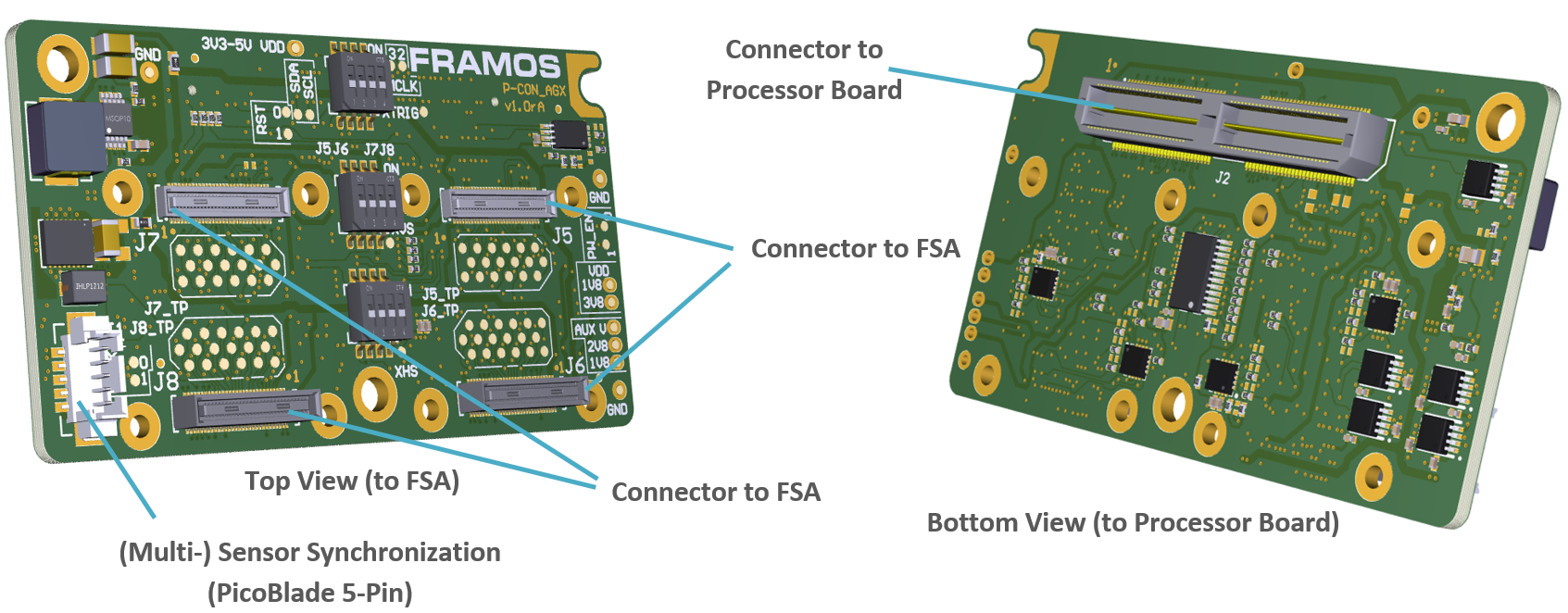
Description of Connectors and Interfaces#
Name |
Description |
Connector Type |
Orientation |
|---|---|---|---|
J1 |
XVS, XHS and XTRIG Signals |
Molex PicoBlade, 5-Pin (53398-0571) |
Pin 1 marked on PCB |
J2 |
PixelMate to Processor Board |
Samtec QTH-060-01-L-D-A |
Pin 1 marked on PCB |
J5 |
PixelMate to FSA (4x MIPI CSI-2 lanes) |
Hirose DF40C-60DS-0.4V(51) |
Pin 1 Printed on PCB next to each connector. |
J6 |
PixelMate to FSA (4x MIPI CSI-2 lanes) |
Hirose DF40H C(4.0)-60DS-0.4V(51) |
Pin 1 Printed on PCB next to each connector. |
J7 |
PixelMate to FSA (4x MIPI CSI-2 lanes) |
Hirose DF40C-60DS-0.4V(51) |
Pin 1 Printed on PCB next to each connector. |
J8 |
PixelMate to FSA (4x MIPI CSI-2 lanes) |
Hirose DF40H C(4.0)-60DS-0.4V(51) |
Pin 1 Printed on PCB next to each connector. |
Table: Connectors on FPA-4.A/AGX-V1A
The Pin 1 markings can be found in the following chapters along with the Pinout, as well as on the PCB in copper or silkscreen layer next to the connector.
Note: All signals are routed from J5, J6, J7, J8 (to FSA) to J2 (to processor), test points and pin row. They follow the signal specification according to the FSA output interface. Control signals going to J1 (I2C, clock, GPIO) are buffered to allow voltage translation.
J1 – XVS, XHS and XTRIG Signals

Type: Molex PicoBlade, 53398-0571
Pinout:
Pin # |
Name |
|---|---|
1 |
1V8_VDD |
2 |
XVS0 |
3 |
XHS0 |
4 |
XTRIG0 |
6 |
GND |
Note: Switches SW1, SW2 and SW3 refer to XVS, XHS and XTRIG signals respectively. When SW1, SW2 and SW3 are off, the corresponding signals XVS0, XHS0 and XTRIG0 are not connected.
J5, J6, J7, J8 - Connectors to Sensor Adapters (FSA)
Connectors |
Type |
|---|---|
J5, J7 |
Hirose DF40C-60DS-0.4V(51) |
J6, J8 |
Hirose DF40HC(4.0)-60DS-0.4V(51) |
Note: The two PixelMate connectors, J5 and J7, feature a compact 1.5 mm height, enabling direct connection of 26.5x26.5mm FSM:GO or classic FSA modules onto the board through J6 and J8.**
Pinout:
Pin |
Name |
Pin |
Name |
Pin |
Name |
Pin |
Name |
|---|---|---|---|---|---|---|---|
1 |
3V8_VDD |
16 |
RST_1 |
31 |
GPIO3(XTRIG0) |
46 |
D_DATA_D_P |
2 |
1V8_VDD |
17 |
NC |
32 |
NC |
47 |
D_CLK_B_N |
3 |
3V8_VDD |
18 |
NC |
33 |
PW_EN_0 |
48 |
D_DATA_D_N |
4 |
1V8_VDD |
19 |
GPIO0(XMASTER0) |
34 |
PW_EN_1 |
49 |
GND |
5 |
2V8_AUX |
20 |
NC |
35 |
GPIO6(SLAMODE0) |
50 |
GND |
6 |
NC |
21 |
I2C_X_SCL |
36 |
GPIO7(SLAMODE1) |
51 |
D_DATA_A_N |
7 |
2V8_AUX |
22 |
I2C_Y_SCL |
37 |
GND |
52 |
D_DATA_B_N |
8 |
NC |
23 |
NC |
38 |
GND |
53 |
D_DATA_A_P |
9 |
1V8_AUX |
24 |
GPIO16(SLAMODE2) |
39 |
MCLK_0 |
54 |
D_DATA_B_P |
10 |
NC |
25 |
GPIO1(XVS0) |
40 |
GPIO4(MCLK2) |
55 |
GND |
11 |
GND |
26 |
NC |
41 |
MCLK_1 |
56 |
GND |
12 |
GND |
27 |
I2C_X_SDA |
42 |
GPIO5(MCLK3) |
57 |
D_DATA_C_P |
13 |
GND |
28 |
I2C_Y_SDA |
43 |
GND |
58 |
D_CLK_A_P |
14 |
GND |
29 |
GPIO2(XHS0) |
44 |
GND |
59 |
D_DATA_C_N |
15 |
RST_0 |
30 |
GPIO10(TENABLE) |
45 |
D_CLK_B_P |
60 |
D_CLK_A_N |
Connector I2C Mapping
The connectors are mapped to specific ports on the I2C multiplexer. Each PixelMate is associated with two I2C lines: the primary line (I2C_X) and the auxiliary line (I2C_Y)
Connector |
I2C_X |
I2C_Y |
|---|---|---|
J5 |
I2C_0 |
I2C_1 |
J6 |
I2C_2 |
I2C_3 |
J7 |
I2C_4 |
I2C_5 |
J8 |
I2C_6 |
I2C_7 |
MIPI CSI-2 Signal Mapping for PixelMate Connectors
PixelMate Pin |
Signal Name |
Signal Name on J5 |
Signal Name on J6 |
Signal Name on J7 |
Signal Name on J8 |
|---|---|---|---|---|---|
P:58 N:60 |
D_CLK_A |
D_CLK_0 |
D_CLK_2 |
D_CLK_4 |
D_CLK_6 |
P:45 N:47 |
D_CLK_B |
D_CLK_1 |
D_CLK_3 |
D_CLK_5 |
D_CLK_7 |
P:53 N:51 |
D_DATA_A |
D_DATA_0 |
D_DATA_4 |
D_DATA_8 |
D_DATA_12 |
P:54 N:52 |
D_DATA_B |
D_DATA_1 |
D_DATA_5 |
D_DATA_9 |
D_DATA_13 |
P:57 N:59 |
D_DATA_C |
D_DATA_2 |
D_DATA_6 |
D_DATA_10 |
D_DATA_14 |
P:46 N:48 |
D_DATA_D |
D_DATA_3 |
D_DATA_7 |
D_DATA_11 |
D_DATA_15 |
J2: Connector to Processor Board#

Label: J2
Type: Samtec QTH-060-01-L-D-A
Pinout:
Pin |
Name |
Pin |
Name |
Pin |
Name |
Pin |
Name |
|---|---|---|---|---|---|---|---|
1 |
D_DATA_0_P |
2 |
D_DATA_2_P |
61 |
D_DATA_10_N |
62 |
D_DATA_14_N |
3 |
D_DATA_0_N |
4 |
D_DATA_2_N |
63 |
GND |
64 |
GND |
5 |
GND |
6 |
GND |
65 |
D_CLK_5_P |
66 |
D_CLK_7_P |
7 |
D_CLK_0_P |
8 |
D_CLK_1_P |
67 |
D_CLK_5_N |
68 |
D_CLK_7_N |
9 |
D_CLK_0_N |
10 |
D_CLK_1_N |
69 |
GND |
70 |
GND |
11 |
GND |
12 |
GND |
71 |
D_DATA_11_P |
72 |
D_DATA_15_P |
13 |
D_DATA_1_P |
14 |
D_DATA_3_P |
73 |
D_DATA_11_N |
74 |
D_DATA_15_N |
15 |
D_DATA_1_N |
16 |
D_DATA_3_N |
75 |
I2C_SCL |
76 |
NC |
17 |
GND |
18 |
GND |
77 |
I2C_SDA |
78 |
NC |
19 |
D_DATA_4_P |
20 |
D_DATA_6_P |
79 |
GND |
80 |
GND |
21 |
D_DATA_4_N |
22 |
D_DATA_6_N |
81 |
2V8_AUX |
82 |
2V8_AUX |
23 |
GND |
24 |
GND |
83 |
2V8_AUX |
84 |
NC |
25 |
D_CLK_2_P |
26 |
D_CLK_3_P |
85 |
NC |
86 |
NC |
27 |
D_CLK_2_N |
28 |
D_CLK_3_N |
87 |
NC |
88 |
MCLK_1 |
29 |
GND |
30 |
GND |
89 |
NC |
90 |
PW_EN_1 |
31 |
D_DATA_5_P |
32 |
D_DATA_7_P |
91 |
MCLK_0 |
92 |
RST_1 |
33 |
D_DATA_5_N |
34 |
D_DATA_7_N |
93 |
PW_EN_0 |
94 |
MCLK_2 |
35 |
GND |
36 |
GND |
95 |
RST_0 |
96 |
NC |
37 |
D_DATA_8_P |
38 |
D_DATA_12_P |
97 |
NC |
98 |
NC |
39 |
D_DATA_8_N |
40 |
D_DATA_12_N |
99 |
GND |
100 |
GND |
41 |
GND |
42 |
GND |
101 |
NC |
102 |
1V8_AUX |
43 |
D_CLK_4_P |
44 |
D_CLK_6_P |
103 |
NC |
104 |
NC |
45 |
D_CLK_4_N |
46 |
D_CLK_6_N |
105 |
NC |
106 |
NC |
47 |
GND |
48 |
GND |
107 |
NC |
108 |
3V3_VDD |
49 |
D_DATA_9_P |
50 |
D_DATA_13_P |
109 |
NC |
110 |
3V3_VDD |
51 |
D_DATA_9_N |
52 |
D_DATA_13_N |
111 |
NC |
112 |
NC |
53 |
GND |
54 |
GND |
113 |
NC |
114 |
NC |
55 |
NC |
56 |
NC |
115 |
GND |
116 |
GND |
57 |
NC |
58 |
NC |
117 |
NC |
118 |
3V3-5V_VDD |
59 |
D_DATA_10_P |
60 |
D_DATA_14_P |
119 |
NC |
120 |
3V3-5V_VDD |
Table: Pinout of FPA-4.A/AGX-V1A connector to NVIDIA Jetson AGX Xavier and AGX Orin
SW1, SW2, SW3: Configuration Switches#
DIP switches SW1, SW2 and SW3 are mainly for interconnecting FSA’s triggering signals (XVS, XHS and XTRIG).
DIP switch SW1 is designated to interconnect XVS pins, DIP switch SW2 is designated to interconnect XHS pins and DIP switch SW3 is designated to interconnect XTRIG pins.

I2C: Access to further Signals
The FPA contains an I2C GPIO extender (TCA6408). It allows the control of further timing uncritical signals through the I2C bus. Each connector is paired with its own dedicated I2C GPIO expander, connected to the I2C_X line. The mapping for I2C_X is as follows:
Connector |
I2C_X |
|---|---|
J5 |
I2C_0 |
J6 |
I2C_2 |
J7 |
I2C_4 |
J8 |
I2C_6 |
While all GPIO expanders share a common address (0x20), they are accessed through different I2C clock and data lines, and the specific I2C line for each connector is identified by the corresponding I2C_X value.
I2C Address [3]_: 0x20
Pinout:
U1
Pin # |
Name |
Pixelmate PIN |
|---|---|---|
P0 |
PW_EN_0 |
33 |
P1 |
PW_EN_1 |
34 |
P2 |
RST_0 |
15 |
P3 |
GPIO0(XMASTER0) |
19 |
P4 |
GPIO6(SLAMODE0) |
35 |
P5 |
GPIO7(SLAMODE1) |
36 |
P6 |
GPIO16(SLAMODE2) |
24 |
P7 |
GPIO10(TENABLE) |
30 |
External Signals & Test Points#


Connector J5: J5_TP and Ungrouped Test Points
Label |
Signal |
Label |
Signal |
|---|---|---|---|
TP18 |
CAM0_RST_0 |
TP62 |
CAM0_GPIO3(XTRIG0) |
TP22 |
CAM0_RST_1 |
TP66 |
CAM0_PW_EN_0 |
TP26 |
CAM0_GPIO0(XMASTER0) |
TP70 |
CAM0_PW_EN_1 |
TP30 |
I2C_0_SCL(SPI_SCK) |
TP74 |
CAM0_GPIO6 |
TP34 |
I2C_1_SCL |
TP78 |
CAM0_GPIO7 |
TP38 |
CAM0_GPIO16(SYS_PW_EN) |
TP82 |
CAM0_MCLK_0 |
TP42 |
CAM0_GPIO1(XVS0) |
TP86 |
GPIO4(MCLK2) |
TP46 |
I2C_0_SDA(SPI_MOSI) |
TP90 |
CAM0_MCLK_1 |
TP50 |
I2C_1_SDA |
TP91 |
GPIO5(MCLK3) |
TP54 |
CAM0_GPIO2(XHS0) |
||
TP58 |
CAM0_GPIO10 |
Connector J6: J6_TP Test Points
Label |
Signal |
Label |
Signal |
|---|---|---|---|
TP19 |
CAM1_RST_0_TP |
TP63 |
CAM1_GPIO3(XTRIG0)_TP |
TP23 |
CAM1_RST_1_TP |
TP67 |
CAM1_PW_EN_0_TP |
TP27 |
CAM1_GPIO0(XMASTER0)_TP |
TP71 |
CAM1_PW_EN_1_TP |
TP31 |
I2C_2_SCL(SPI_SCK)_TP |
TP75 |
CAM1_GPIO6_TP |
TP35 |
I2C_3_SCL_TP |
TP79 |
CAM1_GPIO7_TP |
TP39 |
CAM1_GPIO16(SYS_PW_EN)_TP | TP83 |
CAM1_MCLK_0_TP |
|
TP43 |
CAM1_GPIO1(XVS0)_TP |
TP87 |
CAM1_MCLK1_TP |
TP47 |
I2C_2_SDA(SPI_MOSI)_TP |
||
TP51 |
I2C_3_SDA_TP |
||
TP55 |
CAM1_GPIO2(XHS0)_TP |
||
TP59 |
CAM1_GPIO10_TP |
||
Connector J7: J7_TP Test Points
Label |
Signal |
Label |
Signal |
|---|---|---|---|
TP20 |
CAM2_RST_0_TP |
TP64 |
CAM2_GPIO3(XTRIG0)_TP |
TP24 |
CAM2_RST_1_TP |
TP68 |
CAM2_PW_EN_0_TP |
TP28 |
CAM2_GPIO0(XMASTER0)_TP |
TP72 |
CAM2_PW_EN_1_TP |
TP32 |
I2C_4_SCL(SPI_SCK)_TP |
TP76 |
CAM2_GPIO6_TP |
TP36 |
I2C_5_SCL_TP |
TP80 |
CAM2_GPIO7_TP |
TP40 |
CAM2_GPIO16(SYS_PW_EN)_TP | TP84 |
CAM2_MCLK_0_TP |
|
TP44 |
CAM2_GPIO1(XVS0)_TP |
TP88 |
CAM2_MCLK1_TP |
TP48 |
I2C_4_SDA(SPI_MOSI)_TP |
||
TP52 |
I2C_5_SDA_TP |
||
TP56 |
CAM2_GPIO2(XHS0)_TP |
||
TP60 |
CAM2_GPIO10_TP |
||
Connector J8: J8_TP Test Points
Label |
Signal |
Label |
Signal |
|---|---|---|---|
TP21 |
CAM3_RST_0_TP |
TP65 |
CAM3_GPIO3(XTRIG0)_TP |
TP25 |
CAM3_RST_1_TP |
TP69 |
CAM3_PW_EN_0_TP |
TP29 |
CAM3_GPIO0(XMASTER0)_TP |
TP73 |
CAM3_PW_EN_1_TP |
TP33 |
I2C_6_SCL(SPI_SCK)_TP |
TP77 |
CAM3_GPIO6_TP |
TP37 |
I2C_7_SCL_TP |
TP81 |
CAM3_GPIO7_TP |
TP41 |
CAM3_GPIO16(SYS_PW_EN)_TP |
TP85 |
CAM3_MCLK_0_TP |
TP45 |
CAM3_GPIO1(XVS0)_TP |
TP89 |
CAM3_MCLK1_TP |
TP49 |
I2C_6_SDA(SPI_MOSI)_TP |
||
TP53 |
I2C_7_SDA_TP |
||
TP57 |
CAM3_GPIO2(XHS0)_TP |
||
TP61 |
CAM3_GPIO10_TP |
Other Test Points (Ungrouped)
Label |
Signal |
|---|---|
TP92 |
XVS0_TP |
TP93 |
GND |
TP94 |
GND |
TP95 |
XHS0_TP |
TP96 |
XTRIG0_TP |
Technical Drawing#

Figure: Technical Drawing of FPA-4.A/AGX-V1A
Note: The two PixelMate connectors, J5 and J7, feature a compact 1.5 mm height.