
FSA-FTx/A#
The following chapters provide the relevant technical information for sensor modules (FSM) with native MIPI CSI-2 data output.
A setup with single or multiple sensor modules consists of one to four FSMs, each with an appropriate sensor-specific FSA, and one FPA for the target processor board. Only FSA and FPA designs shown in this chapter are compatible with each other.

While the FRAMOS Sensor Modules (FSM) are designed for maximum efficiency, the FRAMOS Sensor Adapters (FSA) support all current sensors and their specific electronic requirements, from voltage rails to reference clock generation. The goal is to reduce noise and heat generation on the image sensor board by shifting these functions to the FSA. Additionally, users have the option to integrate this circuitry into their own processor board designs, aiming to reduce size and redundancy. All electrical references are created and provided on a per-project basis.
FSA-FTx/A in Detail:
Connects FSM with MIPI CSI-2 Output to FPA
Each FSM has a specific FSA
Functional Blocks:
Signal routing
Voltage generation for image sensor
Power-up sequence for image sensor
Driving frequency generation (oscillator)
EEPROM (config / ID)
Interface Description#
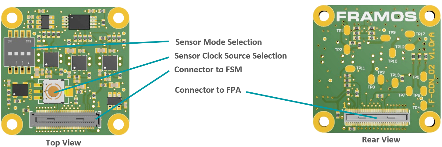
Sensor Mode Selection#
Pos |
Select |
State |
Description |
|---|---|---|---|
1 |
ON OFF |
Enabled / Disabled |
Enable / Disable EEPROM on FSA. Note: It is recommended to be disabled if FSM is equipped with EEPROM. |
2 |
ON OFF |
High / Low |
Select I2C address of sensor, signal depending on sensor type: SLAMODE, SLASEL or SLAMODE1. Please refer to sensor documentation for available signals. |
3 |
ON OFF |
High / Low |
Select I2C address of sensor, signal availability depending on sensor type: SLAMODE2. Please refer to sensor documentation for available signals. |
4 |
ON OFF |
High / Low |
Drive XMASTER pin of FSM (see sensor documentation for details). |
Table: Selection of Sensor Mode on FSA-FTx/A-V1
Sensor Clock Source Selection#
Pos |
Description |
|---|---|
1 |
Clock Provided from FSA (Default) |
2 |
External Clock 1 (MCLK0) |
3 |
External Clock 2 (MCLK1) |
Table: Selection of Sensor Clock Source on FSA-FTx/A-V1
Test Points#

Name |
Signal |
|---|---|
TP1 |
I2C_0_SCL (SPI_SCK) |
TP2 |
I2C_0_SDA (SPI_MOSI) |
TP3 |
IS_MCLK_0 |
TP4 |
IS_RST_0 |
TP5 |
SLAMODE1 |
TP6 |
SLAMODE2 |
TP7 |
IS_GPIO0 (XMASTER0) |
TP8 |
GND |
TP9 |
3V8_VDD |
TP10 |
1V8_VDD |
TP11 |
V_ANA |
TP12 |
V_IF |
TP13 |
V_DIG |
TP17 |
GND |
Table: Test Points on FSA-FTx/A-V1
Connector to FPA#
Type: Hirose DF40C-60DP-0.4V
Name: J1

Pin # |
Name |
Pin # |
Name |
|---|---|---|---|
1 |
3V8_VDD |
2 |
1V8_VDD |
3 |
3V8_VDD |
4 |
1V8_VDD |
5 |
AUX_ANA |
6 |
AUX_DIG |
7 |
AUX_ANA |
8 |
AUX_DIG |
9 |
AUX_IF |
10 |
AUX_V |
11 |
GND |
12 |
GND |
13 |
GND |
14 |
GND |
15 |
RST_0 |
16 |
RST_1 |
17 |
GPIO14 |
18 |
GPIO15(SPI_MISO) |
19 |
GPIO0(XMASTER0) |
20 |
GPIO8 |
21 |
I2C_0_SCL(SPI_SCK) |
22 |
I2C_1_SCL |
23 |
GPIO17(SPI_CS) |
24 |
GPIO16(SYS_PW_EN) |
25 |
GPIO1(XVS0) |
26 |
GPIO9 |
27 |
I2C_0_SDA(SPI_MOSI) |
28 |
I2C_1_SDA |
29 |
GPIO2(XHS0) |
30 |
GPIO10 |
31 |
GPIO3(XTRIG0) |
32 |
GPIO11(FSTROBE) |
33 |
PW_EN_0 |
34 |
PW_EN_1 |
35 |
GPIO6 |
36 |
GPIO7 |
37 |
GND |
38 |
GND |
39 |
MCLK_0 |
40 |
GPIO4(MCLK2) |
41 |
MCLK_1 |
42 |
GPIO5(MCLK3) |
43 |
GND |
44 |
GND |
45 |
D_CLK_1_P |
46 |
D_DATA_3_P |
47 |
D_CLK_1_N |
48 |
D_DATA_3_N |
49 |
GND |
50 |
GND |
51 |
D_DATA_0_N |
52 |
D_DATA_1_N |
53 |
D_DATA_0_P |
54 |
D_DATA_1_P |
55 |
GND |
56 |
GND |
57 |
D_DATA_2_P |
58 |
D_CLK_0_P |
59 |
D_DATA_2_N |
60 |
D_CLK_0_N |
Table: Pinout of FSA-FTx/A-V1, connector to FRAMOS Processor Adapter (FPA)
Note
Colored signals are not routed directly to FSM and might be modified by FSA. All other signals are unmodified and passed through right from the image sensor.
J1: Signal Description to FPA (Part 1/2)#
Pin |
Net Name |
I/O |
Primary function description |
Connected to |
I/O Standard |
I/O State |
I/O DC Characteristic |
|---|---|---|---|---|---|---|---|
1 |
3V8_VDD |
Power |
3.8V Power Supply (Triggers FSA/FSM power-up) |
LDO_ICs, FSM |
3V8_VDD=3.7V-5.1V, max. 0.3A |
||
2 |
1V8_VDD |
Power |
1.8V Power Supply |
LDO_ICs, FSM |
1V8_VDD=1.7V-1.9V, max. 0.3A |
||
3 |
3V8_VDD |
Power |
3.8V Power Supply (Triggers FSA/FSM power-up) |
LDO_ICs, FSM |
3V8_VDD=3.7V-5.1V, max. 0.3A |
||
4 |
1V8_VDD |
Power |
1.8V Power Supply |
LDO_ICs, FSM |
1V8_VDD=1.7V-1.9V, max. 0.3A |
||
5 |
AUX_ANA |
Power |
Not Connected |
(FSM) |
|||
6 |
AUX_DIG |
Power |
Not Connected |
(FSM) |
|||
7 |
AUX_ANA |
Power |
Not Connected |
(FSM) |
|||
8 |
AUX_DIG |
Power |
Not Connected |
(FSM) |
|||
9 |
AUX_IF |
Power |
Not Connected |
(FSM) |
|||
10 |
AUX_V |
Power |
Not Connected |
(FSM) |
|||
11 |
GND |
GND |
Common Ground |
||||
12 |
GND |
GND |
Common Ground |
||||
13 |
GND |
GND |
Common Ground |
||||
14 |
GND |
GND |
Common Ground |
||||
15 |
RST_0 |
IN |
General reset for FSM, resets image sensor (XCLR) |
Reset_IC |
LVCMOS18 (1.8V) |
Normal: High, Reset: Low |
VILmax=0.36V, VIHmin=1.44V |
16 |
RST_1 |
IN |
General reset for FSM |
(Reset_IC) |
LVCMOS18 (1.8V) |
Normal: High, Reset: Low |
VILmax=0.36V, VIHmin=1.44V |
17 |
GPIO14 |
IN |
FSM |
LVCMOS18 (1.8V) |
|||
18 |
GPIO15(SPI_MISO) |
OUT |
FSM |
LVCMOS18 (1.8V) |
VILmax=0.2V, VOHmin=1.6V |
||
19 |
GPIO0(XMASTER0) |
IN |
FSM |
LVCMOS18 (1.8V) |
VILmax=0.36V, VIHmin=1.44V |
||
20 |
GPIO8 |
IN/OUT |
FSM |
LVCMOS18 (1.8V) |
|||
21 |
I2C_0_SCL (SPI_SCK) |
IN |
I2C SCL for EEPROM and FSM |
EEPROM, FSM |
LVCMOS18 (1.8V) |
VILmax=0.54V, VIHmin=1.26V |
|
22 |
I2C_1_SCL |
IN/OUT |
Additional I2C SCL for FSM |
FSM |
LVCMOS18 (1.8V) |
VILmax=0.54V, VIHmin=1.26V |
|
23 |
GPIO17(SPI_CS) |
IN/OUT |
FSM |
LVCMOS18 (1.8V) |
VILmax=0.36V, VIHmin=1.44V |
||
24 |
GPIO16 (SYS_PW_EN) |
IN/OUT |
SYS_PW_EN |
FSM |
LVCMOS18 (1.8V) |
VILmax=0.36V, VIHmin=1.44V |
|
25 |
GPIO1(XVS0) |
IN/OUT |
XVS from/to FSM |
FSM |
LVCMOS18 (1.8V) |
VILmax=0.36V, VIHmin=1.44V |
|
26 |
GPIO9 |
IN/OUT |
FSM |
LVCMOS18 (1.8V) |
VILmax=0.2V, VOHmin=1.6V |
||
27 |
I2C_0_SDA (SPI_MOSI) |
IN/OUT |
I2C SDA for EEPROM and FSM |
EEPROM, FSM |
LVCMOS18 (1.8V) |
VILmax=0.54V, VIHmin=1.26V |
|
28 |
I2C_1_SDA |
IN/OUT |
Additional I2C SDA for FSM |
FSM |
LVCMOS18 (1.8V) |
VILmax=0.54V, VIHmin=1.26V |
|
29 |
GPIO2(XHS0) |
IN/OUT |
XHS from/to FSM |
FSM |
LVCMOS18 (1.8V) |
VILmax=0.36V, VIHmin=1.44V |
|
30 |
GPIO10 |
IN/OUT |
FSM |
LVCMOS18 (1.8V) |
VILmax=0.2V, VOHmin=1.6V |
||
31 |
GPIO3(XTRIG0) |
IN/OUT |
XTRIG for FSM |
FSM |
LVCMOS18 (1.8V) |
VILmax=0.36V, VIHmin=1.44V |
|
32 |
GPIO11(FSTROBE) |
IN/OUT |
FSTROBE from FSM |
FSM |
LVCMOS18 (1.8V) |
VILmax=0.36V, VIHmin=1.44V |
|
33 |
PW_EN_0 |
IN |
PW_EN for FSM |
FSM |
LVCMOS18 (1.8V) |
Normal: High, Down: Low |
VILmax=0.36V, VIHmin=1.44V |
J1: Signal Description to FPA (Part 2/2)#
Pin |
Net Name |
I/O |
Primary function description |
Connected to |
I/O Standard |
I/O State |
I/O DC Characteristic |
|---|---|---|---|---|---|---|---|
34 |
PW_EN_1 |
IN |
Additional PW_EN for FSM |
FSM |
LVCMOS18 (1.8V) |
Normal: High, Pwr Down: Low |
VILmax=0.36V, VIHmin=1.44V |
35 |
GPIO6 |
IN |
(FSM) |
LVCMOS18 (1.8V) |
VILmax=0.36V, VIHmin=1.44V |
||
36 |
GPIO7 |
IN |
(FSM) |
LVCMOS18 (1.8V) |
VILmax=0.36V, VIHmin=1.44V |
||
37 |
GND |
GND |
Common Ground |
||||
38 |
GND |
GND |
Common Ground |
||||
39 |
MCLK_0 |
IN CLK |
Master clock 0 (FSM input clock when SW1 in position 2) |
Rotary Switch |
LVCMOS18 (1.8V) |
VILmax=0.36V, VIHmin=1.44V |
|
40 |
GPIO4 (MCLK2) |
IN/OUT |
FSM |
LVCMOS18 (1.8V) |
VILmax=0.36V, VIHmin=1.44V |
||
41 |
MCLK_1 |
IN CLK |
Master clock 1 (FSM input clock when SW1 in position 3) |
Rotary Switch |
LVCMOS18 (1.8V) |
VILmax=0.36V, VIHmin=1.44V |
|
42 |
GPIO5 (MCLK3) |
IN/OUT |
FSM |
LVCMOS18 (1.8V) |
VILmax=0.36V, VIHmin=1.44V |
||
43 |
GND |
GND |
Common Ground |
||||
44 |
GND |
GND |
Common Ground |
||||
45 |
D_CLK_1_P |
OUT |
MIPI-CSI2 output clock (1, P) |
FSM |
MIPI D-PHY |
||
46 |
D_DATA_3_P |
OUT |
MIPI-CSI2 output data (3, P) |
FSM |
MIPI D-PHY |
||
47 |
D_CLK_1_N |
OUT |
MIPI-CSI2 output clock (1, N) |
FSM |
MIPI D-PHY |
||
48 |
D_DATA_3_N |
OUT |
MIPI-CSI2 output data (3, N) |
FSM |
MIPI D-PHY |
||
49 |
GND |
GND |
Common Ground |
||||
50 |
GND |
GND |
Common Ground |
||||
51 |
D_DATA_0_N |
OUT |
MIPI-CSI2 output data (0, N) |
FSM |
MIPI D-PHY |
||
52 |
D_DATA_1_N |
OUT |
MIPI-CSI2 output data (1, N) |
FSM |
MIPI D-PHY |
||
53 |
D_DATA_0_P |
OUT |
MIPI-CSI2 output data (0, P) |
FSM |
MIPI D-PHY |
||
54 |
D_DATA_1_P |
OUT |
MIPI-CSI2 output data (1, P) |
FSM |
MIPI D-PHY |
||
55 |
GND |
GND |
Common Ground |
||||
56 |
GND |
GND |
Common Ground |
||||
57 |
D_DATA_2_P |
OUT |
MIPI-CSI2 output data (2, P) |
FSM |
MIPI D-PHY |
||
58 |
D_CLK_0_P |
OUT CLK |
MIPI-CSI2 output clock (0, P) |
FSM |
MIPI D-PHY |
||
59 |
D_DATA_2_N |
OUT |
MIPI-CSI2 output data (2, N) |
FSM |
MIPI D-PHY |
||
60 |
D_CLK_0_N |
OUT CLK |
MIPI-CSI2 output clock (0, N) |
FSM |
MIPI D-PHY |
Technical Drawing#
