
IMX530x#
A 24.5MP Global Shutter optical sensor module with the Sony Pregius S image sensor.
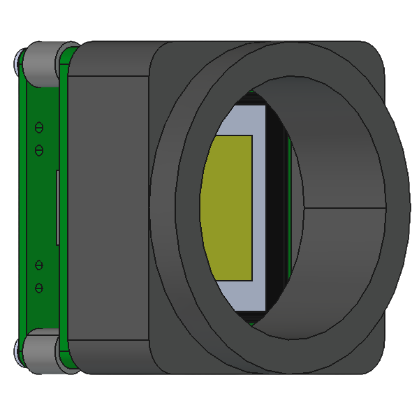
Product Specification - Overview#
Sensor Module#
Type |
Sony IMX530-AAMJ/AAQJ |
|---|---|
Shutter Type |
CMOS Global Shutter |
Technology |
Pregius S (Gen4) |
Spectrum |
Mono or Color (RGB) |
Optical Format |
1.2” |
Pixel Size |
2.74 x 2.74 µm |
Resolution (max.) |
5328 x 4608 |
Framerate (max.)* |
14.7 FPS (4-Lane) |
Bit Depth* |
10/12 bit |
Communication |
I²C (4-wire serial) |
*Platform dependent`
Platform Support (Driver, ISP)#
NVIDIA |
Jetson Family (Orin) |
Supported JP/L4T Versions#
Version |
|
|---|---|
JetPack / L4T |
6.2.1 / 36.4.4 |
6.2 / 36.4.3 |
|
6.1 / 36.4 |
|
6.0 / 36.3 |
Interface Option(s)#
Data Interface |
MIPI CSI-2 v1.2 (D-PHY v2.1) |
Physical Interface |
PixelMate (60 pin) |
Power Supply |
DC (two voltages) |
Power Cons. (3.8V) |
790mW |
Power Cons. (1.8V) |
600mW |
Power Cons. (Max) |
1390mW |
Mechanical Specification#
Dimensions [mm] |
Board: 28 (W) x 28 (D) (H): Lens depending |
Lens Mount |
M12 x 0.5 (var. options) |
Applications#
Barcode scanning
Drones - AGV and AGVs
Industrial robotics
Automated inspection
Environmental#
IP Rating |
Board: None |
Operating Temperature |
-30° to +75°C* |
Storage Temperature |
-40°to +85°C* |
Ambient Humidity |
Max 95% RH, non-condensing |
*Sensor module without lens, check Lens Options for configurations with Lens.
Order Code Scheme/Options#
FSM-IMX530-[CH]-[LM]-[L]-[FS][FD]-[IF]-[MH]-A1Q1#
CH: Chromaticy
C: Color
M: Monochrome
IF: Interface (Mandatory)
PM: PixelMate (60 pin)
Interface Options#
Type (Code) |
PM |
|---|---|
Description |
PixelMate |
FSM Integration |
Default FSM Interface |
Interface Standard |
FRAMOS PixelMateC |
Connector Type |
Hirose DF40C-60 DP-0.4V(51) |
Pin Count [#] |
60 |
Pin Pitch [mm] |
0.4mm |
Locking Style |
Self - locking |
Shielding |
Yes |
Power Supply [V] |
3V8, 1V8 |
Data Lanes /Bandwidth |
4-Lanes, 2.5 Gbps (ea.) |
Mating Connector |
Hirose DF40C-60 DS-0.4V(51) |
Mating Cable(s) |
FMA- FC-150/60 |
Receiver Boards |
Various FPAs |
Pinouts#
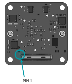
Warning
Pin 1 is identified on the board. Orient accordingly, paying close attention to the pin number in reference to the locater view illustrated below. Failure to align correctly will cause permanent damage.
PixelMate:#
Type: Hirose DF40C-60DP-0.4V(51) |
Pinout |
Pinout |
Pinout |
Pinout |
||||
|---|---|---|---|---|---|---|---|---|
|
1 |
3V8_VDD |
16 |
NC |
31 |
NC |
46 |
D_DATA_3_P |
2 |
1V8_VDD |
17 |
EE_MISO |
32 |
NC |
47 |
NC |
|
3 |
3V8_VDD |
18 |
NC |
33 |
PW_EN |
48 |
D_DATA_3_N |
|
4 |
1V8_VDD |
19 |
NC |
34 |
CRESET_B |
49 |
GND |
|
5 |
NC |
20 |
EE_MOSI |
35 |
NC |
50 |
GND |
|
6 |
NC |
21 |
I2C_SCL |
36 |
NC |
51 |
D_DATA_0_N |
|
7 |
NC |
22 |
NC |
37 |
GND |
52 |
D_DATA_1_N |
|
8 |
NC |
23 |
NC |
38 |
GND |
53 |
D_DATA_0_P |
|
9 |
NC |
24 |
NC |
39 |
MCLK_0 |
54 |
D_DATA_1_P |
|
10 |
NC |
25 |
XVS |
40 |
NC |
55 |
GND |
|
11 |
GND |
26 |
EE_SCK |
41 |
MCLK_1 |
56 |
GND |
|
12 |
GND |
27 |
I2C_SDA |
42 |
NC |
57 |
D_DATA_2_P |
|
13 |
GND |
28 |
NC |
43 |
GND |
58 |
D_CLK_0_P |
|
14 |
GND |
29 |
NC |
44 |
GND |
59 |
D_DATA_2_N |
|
15 |
RST_0 |
30 |
EE_SS |
45 |
NC |
60 |
D_CLK_0_N |
Signal Description#
3V8_VDD I/O Type: Power Function: 3.8V input power line Connected to: LDO_IC I/O Standard: - I/O State: - DC Charact.: 3V8_VDD=3.7V-5.1V, max. 0.3A* |
1V8_VDD I/O Type: Power Function: 1.8V input power line Connected to: LDO_IC I/O Standard: - I/O State: - DC Charact.: 1V8_VDD=1.7V-1.9V, max. 0.3A* |
RST_0 I/O Type: IN Function: Image sensor Reset 0 line (default one) Connected to: Reset_IC I/O Standard: LVCMOS18 I/O State: Normal: High, Reset: Low DC Charact.: VILmax=0.36V, VIHmin=1.44V |
EE_MISO I/O Type: OUT Function: SPI firmware programming SDO line Connected to: Crosslink FPGA and SPI flash I/O Standard: LVCMOS18 I/O State: - DC Charact.: VOLmax=0.4V, VOHmin=1.4V |
EE_MOSI I/O Type: IN Function: SPI firmware programming SDI line Connected to: Crosslink FPGA and SPI flash I/O Standard: LVCMOS18 I/O State: - DC Charact.: VILmax=0.36V, VIHmin=1.44V |
I2C_SCL I/O Type: IN/OUT Function: I2C clock line Connected to: Image sensor; pullup option available but not enabled by default I/O Standard: LVCMOS18 I/O State: - DC Charact.: VILmax=0.36V, VIHmin=1.44V |
XVS I/O Type: IN/OUT Function: Image sensor synchronization signal Connected to: Crosslink FPGA I/O Standard: LVCMOS18 I/O State: - DC Charact.: VOLmax=0.4V, VOHmin=1.4V |
EE_SCK I/O Type: IN Function: SPI firmware programming SCK line Connected to: SPI flash I/O Standard: LVCMOS18 I/O State: - DC Charact.: VOLmax=0.4V, VOHmin=1.4V |
I2C_SDA I/O Type: IN/OUT Function: I2C data line Connected to: Image sensor; pullup option available but not enabled by default I/O Standard: LVCMOS18 I/O State: - DC Charact.: VILmax=0.36V, VIHmin=1.44V |
EE_SS I/O Type: IN Function: SPI firmware programming CS/SS line Connected to: SPI flash I/O Standard: LVCMOS18 I/O State: - DC Charact.: VILmax=0.36V, VIHmin=1.44V |
PW_EN I/O Type: - Function: Power enable pin for Crosslink FPGA power supplies Connected to: LDOs I/O Standard: LVCMOS18 I/O State: - DC Charact.: VILmax=0.36V, VIHmin=1.44V |
CRESET_B I/O Type: IN Function: Reset for Crosslink firmware programming Connected to: Crosslink FPGA I/O Standard: LVCMOS18 I/O State: - DC Charact.: VILmax=0.36V, VIHmin=1.44V |
MCLK_0/1 I/O Type: IN Function: Master clocks for image sensors Connected to: Crosslink FPGA; by default clocks are driven from the oscillator I/O Standard: LVCMOS18 I/O State: - DC Charact.: VILmax=0.36V, VIHmin=1.44V |
D_DATA_0/1/2/3_P/N I/O Type: OUT Function: MIPI-CSI2 data lanes D0-D3 Connected to: corresponding DOPx/DOMx pins on image sensors I/O Standard: MIPI D-PHY I/O State: - DC Charact.: - |
D_CLK_0_P/N I/O Type: OUT Function: MIPI-CSI2 clock pair CLK0 Connected to: DCKP/DCKM pins on image sensor I/O Standard: MIPI D-PHY I/O State: - DC Charact.: - |
* General range of what the connector pin can physically carry, may vary on a case-by-case basis.
I2C Address Configuration (SLAMODE)#
SLAMODE2 |
SLAMODE1 |
SLAMODE0 |
1ˢᵗ I2C Address |
2ⁿᵈ I2C Address |
|---|---|---|---|---|
0 |
0 |
0 |
0x1A |
0x36 |
0 |
0 |
1 |
0x1A |
0x37 |
0 |
1 |
0 |
0x1A |
0x38 |
0 |
1 |
1 |
0x1A |
0x39 |
1 |
0 |
0 |
0x1A |
0x3A |
1 |
0 |
1 |
0x1A |
0x3B |
1 |
1 |
0 |
0x1A |
0x3C |
1 |
1 |
1 |
0x1A |
0x3D |
Note
The FRAMOS driver uses the 1ˢᵗ I2C Address (
0x1A) by default.Users can configure additional SLAMODE signals via DIO (Digital Input/Output) pins from the host to set a unique 2ⁿᵈ I2C Address.
When using multiple sensors on the same host, ensure each sensor is assigned a unique 2ⁿᵈ I2C Address to avoid conflicts.
Power-On Sequencing#
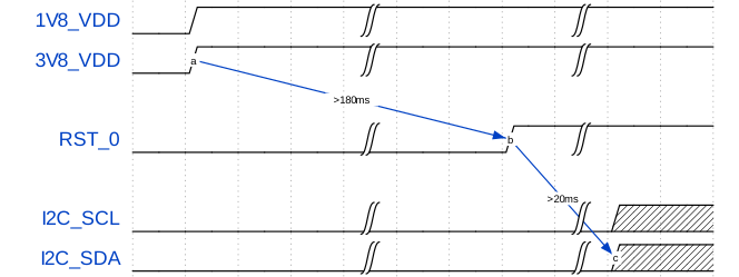
For correct function, the host system must follow the timing below to properly power up or reset the module.
3V8_VDD should be generated after 1V8_VDD, or, ideally at the same time. The RST_0 pin should be low after powering up PixelMate voltage rails > 180 ms.
Legend#
Times and voltages which are represented in the above figure are as follows:
3V8_VDD - 3V8 voltage supply from host
1V8_VDD - 1V8 voltage supply from host
RST_0 - reset signal driven from the host
I2C_SCL - I2C Clock
I2C_SDA - I2C Data
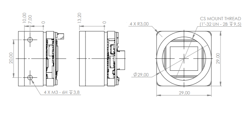
Mechanical Drawings#
The following chapter contains the measured drawings split into the core segments of the product.
Bare Sensor Module
with Mount
All measures refer to the backside of the sensor module PCB and, this way, allow the acquisition of the overall measures. Units of measurement are expressed in milimeters [mm]².
Sensor Module (Bare FSM)#
Interface: PixelMate™#
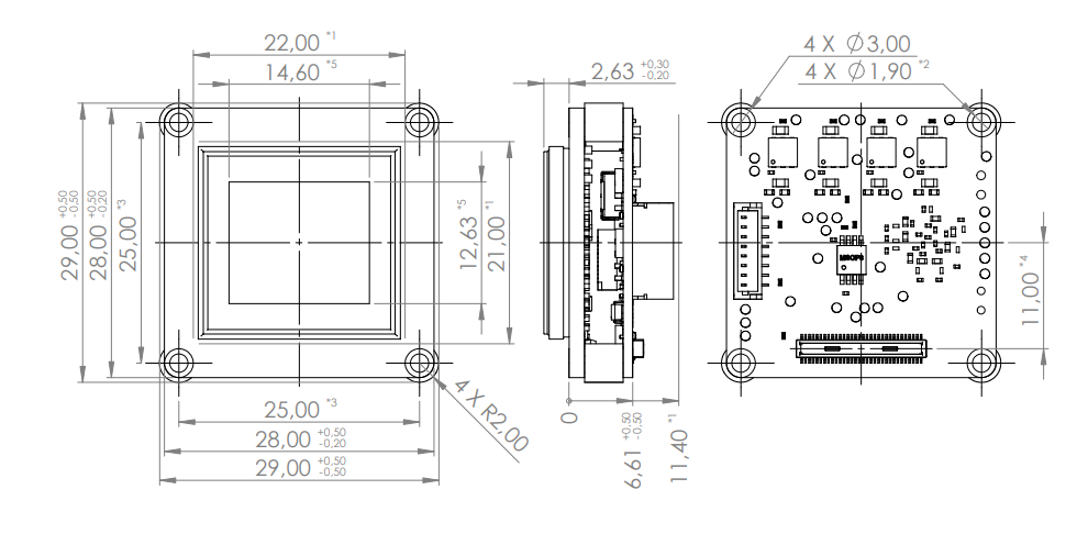
*1 - clearance area
*2 - holes size tolerance +/-0,1mm
*3 - holes position tolerance +/-0,1mm
*4 - connector size & alignment tolerance (X,Y,Z,tilt) +/-0,20mm
*5 - center of active sensor area is aligned with center of sensor board area
sensor active area size & alignment tolerance (X,Y,Z,tilt) +/-0.25mm
2 All mechanical components of the module assembly are subject to form and dimensional tolerances; therefore, sufficient mechanical clearance must be provided during integration, particularly around the lens and lens mount. The placement of electrical components on the PCBs (excluding connectors) may change without prior notice.
FSM with Mount#
PM:#
Platform Compatibility and Software Support#
The FSM:FSA camera module comes with ongoing and off-the-shelf driver support for the latest NVIDIA Jetson Developer Kits and rudimentary ISP tuning working well in office environments. Further compute platforms like NXP, Qualcomm or Raspberry Pi are physically compatible, leveraging our modular adapter ecosystem. Drivers are supported on a per project basis, as well as comprehensive ISP configurations, delivering the best image under any conditions. Implemented sensor and ISP features, as well as the archived performance, are directly related to the capabilities of each processing platform and the BSP maintained by its vendor. GitHub repository for all available driver releases as well as our online documentation for any hardware references.